

According to Kings Research, the U.S. High Bandwidth Memory (HBM) market size was valued at USD 6.65 billion in 2025 and is projected to reach USD 58.40 billion by 2033, representing a CAGR of 31.20% from 2026 to 2033. While the United States does not manufacture these memory chips domestically, it dictates the market's direction by buying, specifying, and funding the technology. This exponential expansion highlights a massive shift in hardware architecture.
Artificial intelligence processing requires massive data streams. Silicon processors execute mathematical calculations at blistering speeds. Traditional motherboards fail to deliver data fast enough to keep these processors busy. This creates a severe data traffic jam. Engineers call this the memory wall. To bypass this barrier, semiconductor companies developed specialized packaging architectures. They move the data storage directly next to the processing cores. This proximity eliminates latency. It allows graphics processing units to operate at maximum efficiency. Federal agencies and cloud service providers recognize this technology as critical infrastructure. Deploying these advanced silicon packages requires vast capital investments, making American cloud giants and national laboratories the primary drivers of global demand.
What Is High Bandwidth Memory?
What is high bandwidth memory and why is it important for AI? High bandwidth memory is an advanced silicon packaging architecture utilizing three-dimensional stacked DRAM placed directly alongside the processor. It is critical for artificial intelligence because it provides massive data throughput with minimal latency, bypassing severe data transfer limits found in conventional planar circuit boards.
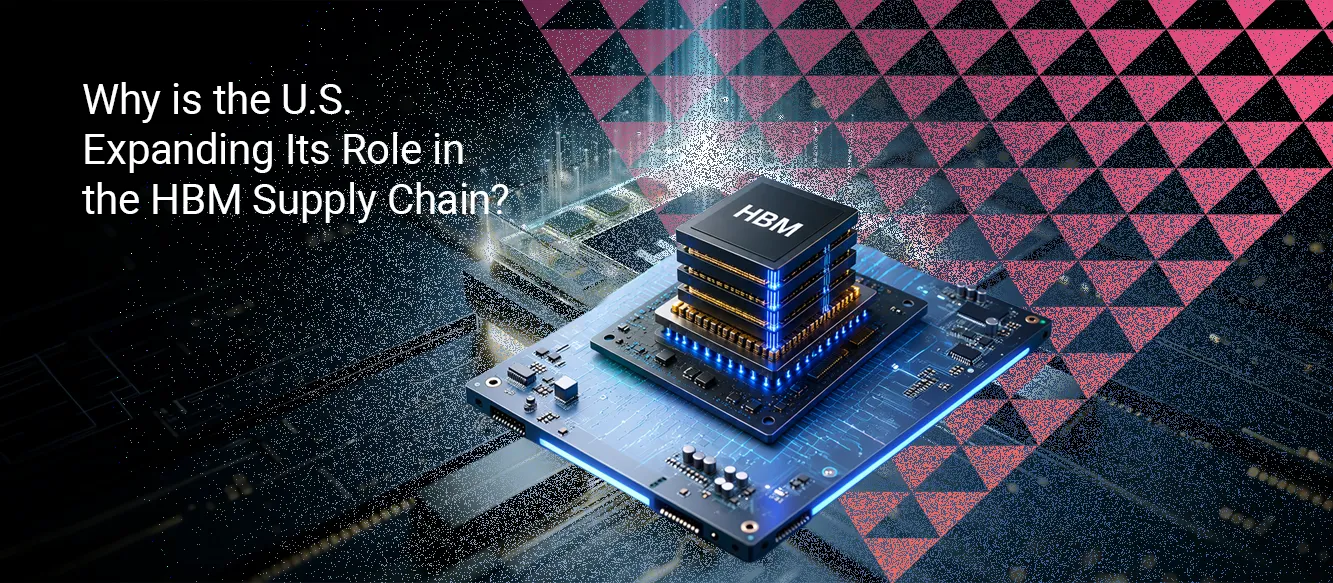
Standard memory chips sit flat on a printed circuit board. They connect to the processor through long copper lines. Advanced packaging stacks multiple memory chips vertically. This vertical tower sits on a specialized silicon base called an interposer. The processor also sits on this exact same interposer. Microscopic wires inside the interposer connect the memory tower directly to the processor. This layout drastically shortens the physical distance electrical signals must travel. Shorter distances equal faster data transfer. Faster data transfer equals faster artificial intelligence model training.
This physical arrangement creates a massive highway for information. Data flows freely between the storage cells and the computing cores. Engineers designed this system specifically for workloads requiring continuous data feeds. Standard memory forces data through a narrow pipe. Stacked memory opens thousands of wide pipes simultaneously. This architectural shift enables modern supercomputers to function properly. Without this hardware advancement, artificial intelligence scaling would halt completely. Software developers rely entirely on hardware engineers to solve these physical constraints.
Why Does Memory Bandwidth Limit AI Performance Today?
Artificial intelligence models rely entirely on vast datasets. Large Language Models utilizing the Transformer architecture demand constant data access for every generated token. The processor must retrieve billions of parameters from storage continuously. When a processor requests data, it must wait for electrical signals to travel across the physical distance of the circuit board. This physical distance creates latency. Over recent years, computational capabilities scaled exponentially. Data transfer speeds lagged behind. This mismatch leaves expensive graphics processing units idle while waiting for information.
In Census Bureau surveys conducted between December 2025 and May 2026, the share of businesses reporting AI use in the prior two weeks ranged from 17 to 20 percent. Expanding this usage requires vast infrastructure capable of handling enterprise workloads. Enterprise applications require real-time responses. A delayed response ruins the user experience. Traditional hardware architectures lack the physical bandwidth required to deliver parameters instantly.
Modern models require thousands of graphics processing units working simultaneously. These units must share data across the cluster constantly. If the local memory fails to deliver data quickly, the entire cluster slows down. Network interconnects also depend on fast local memory to buffer incoming data streams. A slow memory subsystem creates a ripple effect across the entire data center. A standard dual-inline memory module provides limited connection pins. This physical bottleneck restricts the total volume of data moving per clock cycle. Eliminating this bottleneck requires entirely new hardware paradigms. Vertical stacking provides thousands of parallel connection pins. These parallel channels deliver terabytes of data every second. This massive throughput allows the processor to evaluate billions of neural weights instantly.
What Happens When Compute Outpaces Memory?
When a processor lacks adequate data delivery, system utilization plummets. Data centers measure efficiency by evaluating how often a processor actively executes mathematical operations. A system constrained by sluggish data delivery forces the processing unit to pause operations. These pauses waste electrical energy. They also extend computing time significantly. Wasted electricity costs cloud providers millions of dollars annually.
Data centers represent massive capital investments. Every idle second reduces the return on investment. Hyperscale operators monitor processor utilization obsessively. They deploy advanced software schedulers to keep the hardware busy. However, software optimization reaches a hard physical limit. When the hardware simply lacks the bandwidth to move data, software tweaks fail to improve performance. The system requires a fundamental hardware upgrade.
The U.S. Department of Energy (DOE) encountered these exact challenges while developing exascale supercomputing infrastructure. In May 2022, DOE deployed the Frontier supercomputer at Oak Ridge National Laboratory, where this system achieved an unprecedented 1.1 exaflops of performance. At this scale, executing massive scientific simulations requires data throughput far exceeding traditional memory limits. Deployed in 2024 at Lawrence Livermore National Laboratory, El Capitan held the world's fastest ranking until June 2026, performing more than 2.79 exaflops per second. The system was built under a USD 600 million NNSA contract signed in 2019 and relies on a 3D chiplet processor design to tightly integrate computing cores. By implementing these advanced high-density architectures, these systems maintain high processor utilization. This ensures multi-million-dollar computing clusters operate at peak efficiency rather than idling in wait states. Fast data delivery allows researchers to simulate complex molecular interactions smoothly.
What Makes High Bandwidth Memory Architecturally Different from Traditional DRAM?
Traditional memory modules sit in dedicated slots far away from the processor. They connect via long traces printed onto the motherboard. This standard layout limits the number of connection pins available for data transfer. Electrical resistance along these long copper traces degrades signal integrity. Engineers must boost the voltage to push signals across the board safely. Higher voltage generates excess heat and consumes massive amounts of electricity.
Advanced silicon packaging solves this physical constraint completely. Engineers stack multiple silicon dies vertically. They connect these vertical layers using Through-Silicon Vias. These microscopic copper channels run directly through the silicon layers. They create thousands of vertical data pathways. The stacked module then sits on a silicon interposer directly adjacent to the processing unit. This proximity drastically reduces the physical distance electrons must travel. The interposer contains microscopic routing wires. These wires provide thousands of wide data channels.
The manufacturing process requires extreme precision. Foundries use chemical-mechanical polishing to thin the silicon wafers perfectly. They use plasma etching to drill the microscopic vias. They fill these vias with conductive copper. They align the vertical layers with microscopic precision. They bond the layers together using thermal compression. This complex sequence creates a dense, highly efficient data storage tower.
The evolution of this architecture has led to massive generational leaps in throughput. Because capacity, stack height, and publication dates vary depending on the specific manufacturer implementation or standards body release, the following table strictly compares the verified interface and speed specifications of the two most current advanced memory generations:
|
Memory Generation |
Interface Width |
Pin Speed |
Bandwidth per Stack |
|
HBM3E |
1024-bit (Micron) |
>9.2 Gb/s (Micron) |
896 to 1,280 GB/s (Kings Research) / >1.2 TB/s (Micron) |
|
HBM4 |
2048-bit (JEDEC April 2025) |
Up to 8 Gb/s (JEDEC) / >11 Gb/s (Micron) |
Up to 2 TB/s (JEDEC) / >2.8 TB/s (Micron) |
How Are AI Accelerators Redefining Memory Requirements in the U.S.?
Modern artificial intelligence relies entirely on specialized accelerators. Graphics Processing Units and Tensor Processing Units handle thousands of mathematical operations simultaneously. To feed these parallel cores, the system requires massive data throughput. Standard enterprise servers use central processing units designed for sequential tasks. Sequential tasks require minimal data bandwidth. Parallel tasks require extreme data bandwidth.
Federal agencies prioritize this exact hardware dependency. The U.S. National Science Foundation (NSF) invests over USD 700 million each year across AI research, education, and infrastructure. Translating this advanced research into viable commercial applications requires robust hardware capable of sustaining extreme workloads.
Inference workloads demand different specifications compared to training workloads. Training requires moving terabytes of raw data continuously to adjust neural weights. This phase takes months to complete. Inference requires holding the finished model parameters in fast local storage to respond to user prompts instantly. Both scenarios demand extreme data transfer speeds. Vertically stacked modules fulfill these requirements by providing thousands of wide data channels directly to the processing cores. This allows developers to build larger, more accurate models. The hardware sets the boundary for software capabilities. Expanding the hardware boundary directly accelerates software sophistication.
How Does High Bandwidth Memory Improve Real-World AI Workload Efficiency?
The primary advantage of advanced packaging is time reduction. Shorter processing times translate directly into financial savings for cloud service providers. Electricity costs represent a massive expense for data centers. Completing a computational workload faster allows the system to enter low-power states sooner. This reduces the total energy consumed per calculation.
The macroeconomic impact of these efficiency gains is highly measurable. The U.S. Bureau of Labor Statistics (BLS) published findings showing that nonfarm business sector labor productivity increased 0.3 percent during the first quarter of 2026. Advanced hardware infrastructure provides a foundation that can support these broader macroeconomic productivity trends. Equipping data centers with advanced silicon allows enterprises to automate complex workflows rapidly.
Worked Example: Training Time Reduction via Advanced Hardware
- Inputs:
- Dataset Size: 500 Terabytes
- Standard DDR5 Bandwidth: 64 Gigabytes per second
- HBM3E: approximately 1.2 TB/s per stack
- Worked Figures:
- Theoretical Data Transfer Time (DDR5): 7,812 seconds (approx. 130 minutes)
- Theoretical Data Transfer Time (Advanced Stacked): 416 seconds (approx. 7 minutes)
- Efficiency Gain: Data movement occurs 18.75 times faster per cycle.
This worked example models a single data transfer pass across a 500 terabyte dataset, saving over two hours of transfer time on a single pass. Across large-scale AI workloads where data and neural weights are accessed continuously over thousands of iterations, these per-pass savings compound substantially to keep processing clusters operating efficiently.
Why Are Hyperscale Data Centers Driving Rapid Adoption of HBM?
Cloud providers build massive infrastructure clusters known as AI factories. These facilities house tens of thousands of accelerators working in tandem. To scale effectively, every individual server node must operate without data bottlenecks. A single bottleneck slows the entire cluster.
The financial commitment to this infrastructure continues growing rapidly. In the first half of 2025, Apollo chief economist Torsten Slok calculated that data center investment contributed as much to U.S. GDP growth as consumer spending. Consumer spending usually drives the American economy. Seeing data center construction match this output highlights an unprecedented infrastructure boom.
Cloud providers demand continuous improvements in data throughput to support increasingly complex parameter models. Without vertical integration, scaling these facilities would require unmanageable amounts of physical space and electricity. Vertically stacked silicon allows cloud providers to pack massive computing power into standard server racks. This density maximizes the return on real estate and power provisioning.
What Is Driving Supply Constraints in the HBM Ecosystem?
Why is there a shortage of HBM? Supply constraints exist because cloud provider demand massively exceeds current manufacturing capacity. Fabricating stacked chips requires specialized packaging equipment and extended production cycles. Achieving defect-free microscopic connections presents severe yield challenges, limiting overall industry output volumes globally.
This supply bottleneck is further intensified by extreme geographical concentration in manufacturing. According to RAND, South Korea is expected to hold 78 percent of global HBM production capacity by the end of 2026, with Taiwan holding 10 percent, Japan 8 percent, and China 4 percent.
The U.S. Census Bureau M3 survey tracked unfilled orders for computers and electronic products reaching $152.9 billion in March 2026 (excluding semiconductor manufacturing). According to Kings Research, this bottleneck translates into average delivery lead times of 12 to 18 months, with prices rising 20 to 40 percent year over year. Standard memory typically takes roughly one month to fabricate. Vertically stacked modules typically require several additional months for testing, aligning, bonding, and packaging. This extended manufacturing timeline creates inherent supply chain friction. If a single microscopic via fails during the bonding process, the entire silicon stack becomes defective. Foundries must throw away the ruined chips. This low yield rate keeps prices high and availability low. Building new foundries typically takes three to five years. Thus, supply remains highly constrained despite massive financial investments from semiconductor manufacturers.
How Are Semiconductor Leaders Expanding HBM Production Capacity?
To address supply constraints, leading semiconductor manufacturers are committing billions of dollars toward capacity expansion. Market share remains tightly held: according to TrendForce data reported by RAND, at the end of 2025, SK hynix held 57 percent of the global HBM market by revenue, while Samsung and Micron held 22 percent and 21 percent, respectively. Micron stands as the only U.S.-headquartered HBM producer, entering high-volume production of its HBM4 part in March 2026. However, Micron manufactures its HBM chips in Taiwan and Japan, while its domestic expansion in Boise, Idaho focuses on standard DRAM.
To establish advanced packaging infrastructure on American soil, international suppliers are expanding into the U.S. with federal support. The U.S. Department of Commerce awarded SK hynix up to $458 million in direct funding to build a high-bandwidth-memory packaging and research facility in West Lafayette, Indiana. This project supports $3.87 billion in expected capital expenditure by SK hynix, with an additional $500 million available in federal loans. Mass production at the Indiana facility is expected to begin in the second half of 2028.
The federal government heavily incentivizes this domestic expansion. The CHIPS and Science Act provides the Department of Commerce with $52.7 billion to boost domestic manufacturing and research. Within this budget, the Department of Commerce oversees $39 billion in direct incentives to encourage investment in facilities and equipment on U.S. soil, though 2026 is the last financial year in which Commerce is due to receive this funding. Expanding capacity involves purchasing specialized bonding equipment, extreme ultraviolet lithography machines, and automated testing robots. The coordinated effort between corporate investment and federal subsidies aims to build out this critical downstream footprint.
Companies use this funding to build cleanrooms, train technicians, and develop robust domestic supply chains for raw materials. Securing this production domestically protects the American technology sector from global shipping disruptions.
What Role Do Advanced Packaging Technologies Play in HBM Growth?
Fabricating the memory chips represents only a fraction of the challenge. Connecting them to the processor requires advanced packaging. Engineers use a silicon interposer as a foundational layer. The processor and the stacked memory modules sit together on this interposer. Microbumps create electrical connections between the chips and the interposer circuitry.
This packaging complexity drives entirely new equipment subsectors. Recognizing this critical technical layer, in November 2023, NIST set out a vision for approximately USD 3 billion in funding for the National Advanced Packaging Manufacturing Program (NAPMP) to drive U.S. leadership in advanced packaging. In August 2026, the Government Accountability Office reported that Commerce had canceled or paused NAPMP awards. Thermal management remains a critical focus within this packaging layer. Stacking silicon dies traps heat. Equipment manufacturers develop specialized materials and liquid cooling solutions to dissipate this thermal energy safely.
Foundries invest billions into packaging research. The substrate materials must handle extreme temperature fluctuations. Different materials expand at different rates when heated. Engineers must perfectly match the thermal expansion coefficients of the silicon chips and the interposer. Failing to match these coefficients causes the package to crack during operation. Packaging reliability directly dictates the lifespan of the accelerator. As transistor density increases, mastering these packaging techniques becomes the primary differentiator for advanced semiconductor production technologies. Companies that master thermal dynamics win massive contracts from hyperscale cloud providers.
How Are Emerging Memory Alternatives Challenging or Complementing HBM?
While vertical stacking dominates high-end accelerators, engineers constantly explore alternative architectures. Low Power Double Data Rate (LPDDR) memory, traditionally used in smartphones, sees increasing adoption in edge computing devices. Edge devices run smaller inference models locally. They require extreme power efficiency rather than maximum bandwidth.
Federal research initiatives actively fund these explorations. The CHIPS Research and Development Office manages $11 billion to develop a robust domestic research ecosystem. This funding ensures U.S. engineers possess the resources required to investigate experimental architectures, photonic interconnects, and novel substrate materials. Hybrid architectures also show immense promise. These systems combine vertical stacks for immediate processing with large pools of Compute Express Link attached memory for secondary storage. This tiered approach lowers the overall system cost while maintaining high performance for critical operations. Diversifying the hardware ecosystem prevents over-reliance on a single manufacturing technique.
How Is Policy and Federal Investment Strengthening U.S. Memory Leadership?
The federal government treats semiconductor manufacturing and its associated packaging ecosystems as critical infrastructure. By funding research and driving massive demand through national laboratory procurements, federal policies ensure the United States maintains a dominant position in hardware development and integration. Equipping the workforce to utilize these advanced technologies requires targeted investment.
Legislators introduced the NSF AI Education Act of 2025, which has since passed the House Science Committee, to expand artificial intelligence education and workforce training programs at the National Science Foundation. This bill supports scholarships and professional development to build essential skills among students and workers. Additionally, the NSF TechAccess: AI-Ready America initiative aims to boost readiness in every U.S. state. The NSF anticipates awarding up to USD 5 million per year for a national coordination lead, USD 1 million per year for three years to each state-level coordination hub, and between USD 5 million and USD 10 million per AI-Ready Catalyst Award competition.
By bridging the gap between hardware capabilities and workforce readiness, federal policy strengthens the entire computing ecosystem. A highly trained workforce ensures that newly constructed data centers operate flawlessly. Educational investments guarantee a steady pipeline of engineers capable of designing the next generation of silicon architectures. These investments target community colleges and vocational schools alongside major universities. Developing a skilled technician workforce ensures foundries operate smoothly. Technicians must understand cleanroom protocols, vacuum systems, and lithography maintenance. Building the physical factories solves only half the challenge. Staffing these factories with highly trained professionals secures long-term operational success. The federal strategy encompasses the entire technology lifecycle.
What Is the Future Outlook for AI Memory Infrastructure in the U.S.?
The roadmap for silicon architectures points toward aggressive scaling. The JEDEC Solid State Technology Association published the HBM4 specification in April 2025. Engineers currently finalize specifications for next-generation interfaces. Future iterations will expand the data bus width and increase clock speeds, doubling total bandwidth per package. Industry projections indicate direct integration onto the processor die itself. This approach bypasses the interposer entirely. To monitor these AI infrastructure growth trends, detailed capacity forecasts, and market trajectory analysis, industry professionals track metrics in the comprehensive Kings Research U.S. High Bandwidth Memory market report. The hardware foundation built today dictates the computational limits of tomorrow.
Frequently Asked Questions
What is the main advantage of HBM over conventional DDR memory?
Compared with standard DDR modules, HBM provides exponentially higher data bandwidth and lower latency by utilizing vertical silicon stacking and thousands of microscopic connections directly adjacent to the processing unit.
Why is HBM expensive?
It requires highly complex manufacturing processes. These processes include Through-Silicon Vias, advanced interposers, and precise thermal packaging. These complex steps reduce manufacturing yield and increase overall production costs.
Can HBM replace traditional memory?
It remains cost-prohibitive for standard consumer laptops or basic enterprise servers. Its extreme performance makes it primarily suited for high-performance computing and complex machine learning workloads.
What industries benefit most from HBM?
Cloud service providers, financial modeling firms, scientific research laboratories, and pharmaceutical companies utilize this technology. They run complex simulations and massive artificial intelligence models flawlessly.
What is the difference between HBM3 and HBM4?
HBM4, published in April 2025, expands the physical connection interface from 1024 bits to 2048 bits. This effectively doubles the data transfer rate while maintaining strict power efficiency requirements.
To access complete statistical breakdowns and comprehensive capacity forecasts, explore the full Kings Research report today.