
Inquire Now
Key Strategic Points
The High Bandwidth Memory (HBM) market refers to the ecosystem of volatile storage technology with wide applications across AI/ML workloads, high-performance computing, and high-end graphics applications. The high bandwidth, and lower latency property of HBMs drives their adoption across cloud computing, and hyperscale data center infrastructure in the U.S. This is driving manufacturers to scale production and develop high-capacity, low-latency memory solutions for next-generation computing applications.
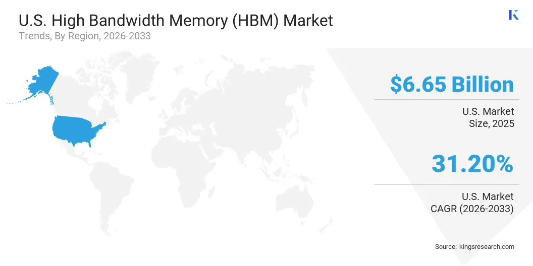
The U.S. High Bandwidth Memory (HBM) market size was valued at USD 6.65 billion in 2025 and is projected to reach USD 58.40 billion by 2033, representing a CAGR of 31.20% over the forecast period (2026-2033). HBMs are high-performance, high-throughput, massive-bandwidth architecture memory chips that are made by stacking DRAM dies on a base die to deliver memory bandwidth. The process results in the generation of a memory of high bandwidth, which is widely adopted across AI accelerators and high-performance computing (HPC) applications. Furthermore, the process is enabling DRAM manufacturers to allocate DRAM facilities towards HBM production owing to the high revenue per die yield of HBMs.
The evolution of AI memory chips to address high-speed data processing for AI training and inference is driving demand for HBM in the U.S. The integration of HBM with AI logic chips eliminates data bottlenecks, which enables large-volume, high-speed data transmission. The adoption of high-performance computing further positions HBM in a transformative state that addresses the critical bottleneck of memory bandwidth. HBM leverages advanced 2.5D and 3D architectures which enables delivery of massive throughput, high-power efficiency, improved thermal management, and scalability for next-generation workloads. The data transfer rate doubling to 16 Gb/s by HBM4E and enhanced reliability and flexibility position HBM as a critical part of AI, HPC, and data-intensive applications.
Key players operating in the market include SK Hynix Inc., Samsung Electronics, and Micron Technology, Inc., which capture more than 95% market share in 2026. The HBM market ecosystem is further driven by companies including NVIDIA, AMD, Intel Corporation, Rambus Inc. and others, which provide hardware and software solutions including AI accelerators, memory interface IP, HBM memory controllers, or high-speed interconnect technologies that drive HBM adoption across AI, HPC, and data center applications.
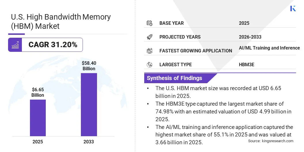
Processors in the current generation are held back by their inability to access data quickly which hampers their adaptability in handling AI workloads, which include enormous datasets processing. The training of AI models by a GPU requires constant access to billions of data points, which results in memory delay, emphasizes processor idling and data waiting. HBM provides increased bandwidth (e.g. HBM3 delivers speeds up to 6.4 Gb/s) which reduces latency through stacked architecture, and improves power efficiency. Furthermore, their compact form is favorable for space-constrained applications.
The rise in hyperscale investments and high-performance computing applications in the U.S. drives the market growth of HBM for advanced GPUs and AI applications. Market players including Samsung Electronics, SK Hynix, and Micron Technology collectively capture a significant share of the global HBM market. The companies have directed research and production towards developing higher architectures of HBM to address rising demand for AI-optimized memory solutions.
Moreover, the exponential growth of AI accelerators across AI technology developers and cloud service providers requiring high-bandwidth memory to run computationally intensive machine learning and generative AI workloads further drives market growth. AI accelerators leverage predictable data access patterns through hardware techniques such as data prefetching to provide high memory bandwidth and low latency required to sustain these workloads efficiently. Companies including NVIDIA and Google are relying on HBM for their H100 and TPU v5p to feed massive transformer models.
DRAM supply constraints are providing the suppliers pricing power in HBM market. The sharp rise in prices is attributed to limited supply, shifting manufacturing capacity allocation from DRAM towards high-bandwidth memory, and surging AI and data center demand. HBM consumes a disproportionate amount of advanced DRAM wafer capacity, which further involves extreme precision stacking process that is difficult to replicate or scale consistently. This results in lower yield and leads to limited supply.
Furthermore, the ramping up of HBM production capacities by SK Hynix, Samsung, and Micron, is leading to an average lead time of 12-18 months in deliveries, further causing supply concentration and limited production. Hence, market players gain significant pricing power, which leads to scaling up of prices by 20-40% year-over-year. The expansion of AI infrastructure reshapes this supply, pricing dynamics and investment strategies across the U.S. semiconductor industry. AI model training, deployments and inference workloads require high memory, which further increases reliance on high-performance GPUs that process large volumes of high-speed data to train and operate complex AI models.
To address the challenge and accelerate next-generation HBM production, manufacturers are expanding capacity, prioritizing AI-focused memory over conventional DRAM, adopting alternative technologies, and increasing investments in advanced packaging technologies.
The transition to higher HBM generations is attributed to the higher bandwidth delivery compared to conventional DDR memory. Each new HBM generation is designed to deliver roughly double the bandwidth of its predecessor. For instance, HBM3E delivers 896–1,280 GB/s bandwidth per stack with up to 48 GB capacity in 16-high configurations, which acts as the baseline for AI accelerators in 2026. This leads to lower latency, improved energy efficiency, and higher compute performance, resulting in faster AI model training and inference and further extending its applicability in next-generation AI accelerators and high-performance computing (HPC) workloads.
The deployment of AI models across commercial and industrial enterprises is further poised to fuel the demand for higher bandwidth memory chips. The demand is anticipated to be fueled by AI model requirements for higher memory bandwidth exceeding 1,000 GB/s to handle massive AI/ML workloads where HBM facilitates efficient data transfer between memory and processing units including GPUs, or AI accelerators.
|
Segmentation |
Details |
|
By Type |
HBM2E, HBM3, HBM3E, HBM4, Others |
|
By Application |
AI/ML Training and Inference, High-Performance Computing (HPC), Gaming and Graphics, Others |
|
By Country |
U.S. |
The U.S. is designated as a premier hub for data centers and artificial intelligence (AI) computing infrastructure which fuels the market growth of high-performance computing hardware required to drive the workloads. The development of advanced LLMs and increasing Generative AI applicability across the commercial and industrial landscape of the U.S. further fuels high capacity and high-bandwidth memory chips. Commercial business entities are operationalizing AI by transitioning it beyond pilot projects and embedding it directly into the core business operations. This is driving the demand for high performance memory requirements, leading to growth avenues across the U.S. HBM market.
Key players operating in the market are expanding production capacities to strengthen their market position and capture a larger share of the growing AI memory market. Companies are further entering strategic partnerships with technology providers to accelerate HBM technology development, commercialization and secure long-term supply agreements to mitigate supply constraints and ensure uninterrupted access to high-bandwidth memory amid rising demand.
Frequently Asked Questions

Faizy brings over four years of experience in market research and consulting, with a proven ability to support strategic engagements across diverse industries and business environments. His work focuses on understanding complex market structures, identifying emerging opportunities, and translating research findings into clear, commercially relevant insights. With strong analytical capabilities and a structured approach to problem-solving, he evaluates industry trends, competitive landscapes, customer dynamics, and evolving business models. His expertise encompasses market research, competitive intelligence, market sizing and forecasting, industry assessment, company benchmarking, and strategic analysis. Faizy combines technical proficiency with a strong research orientation, enabling him to interpret both qualitative and quantitative information effectively. He has contributed to projects that help organizations assess growth potential, strengthen market positioning, and evaluate strategic priorities. His adaptable approach allows him to work across sectors while maintaining a consistent focus on accuracy, relevance, and delivering insights that support informed decision-making for clients and stakeholders.
Habi is a seasoned research and consulting leader with renowned experience in guiding clients on strategic growth and transformation initiatives across global markets. He has led high-performing research teams that deliver actionable insights on market expansion, M&A strategies, opportunity assessment, new business development, and product launches. His project portfolio spans large petrochemical producers, electronic device manufacturers, lubricants companies, and other leading enterprises across diverse industrial and consumer sectors. He currently heads the research department at Kings Research, where he is responsible for setting the research agenda, mentoring analysts, and ensuring client-ready deliverables that support executive decision-making. With extensive experience in market intelligence, strategic research, and consulting, Habi brings a strong understanding of evolving industry dynamics, competitive landscapes, emerging opportunities, and business growth challenges. His expertise includes developing research frameworks, translating complex market data into actionable strategic recommendations, and working closely with senior stakeholders to address critical business questions. He has also contributed to building research capabilities, strengthening analytical methodologies, and driving a culture of quality and insight-led decision-making within research teams. His cross-industry exposure enables him to connect market trends with broader business implications and provide perspectives that help organizations identify opportunities, mitigate risks, and make informed strategic decisions.