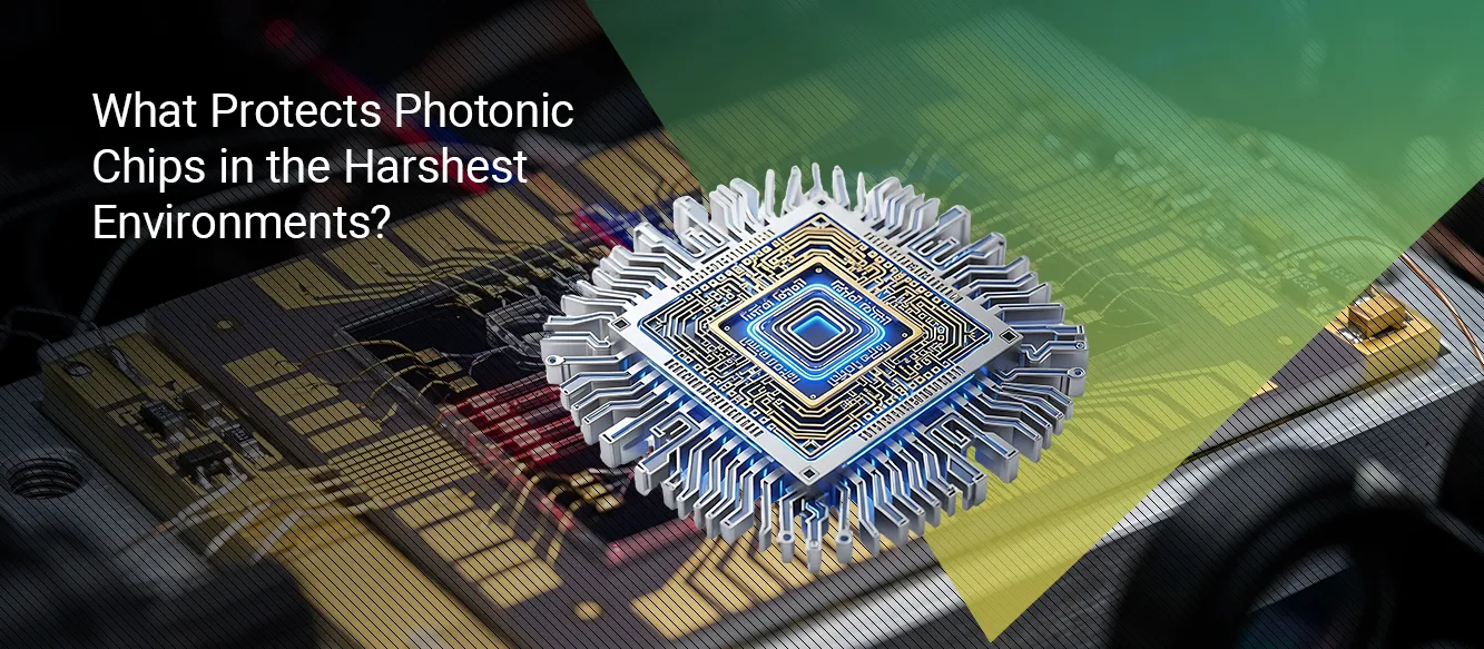
Photonic integrated circuits present immense value for optical sensing and communications, relying on light rather than electrical signals to process information. Deploying these optical chips in extreme environments presents severe engineering hurdles. Extreme temperatures, high radiation levels, mechanical stress, and vacuum conditions degrade optical connections and packaging materials. Reliable operation depends heavily on stable fiber-to-chip alignment, advanced material selection, comprehensive environmental testing, and rigorous application qualification.
Global valuation for the photonic integrated circuits market reached USD 15.99 billion in 2025. Projections indicate growth to USD 77.24 billion by 2033, expanding at a 22.17% CAGR, according to Kings Research. Optical chips utilize light for sensing and communications, offering high bandwidth and immunity to electromagnetic interference. While laboratory performance remains impressive, deploying these systems in harsh conditions requires robust materials, stable interfaces, and repeatable manufacturing processes.
What Are Photonic Integrated Circuits?
Photonic integrated circuits integrate multiple optical components onto a single semiconductor substrate. Similar to how electronic integrated circuits combine transistors, capacitors, and resistors to manage electrical current, optical chips combine lasers, modulators, detectors, and waveguides to manipulate photons. This integration allows devices to generate, process, route, and detect light signals within a microscopic footprint. Silicon, indium phosphide, and silicon nitride serve as the primary foundational materials for these platforms, each offering distinct advantages for specific wavelengths and applications. Silicon provides excellent transparency for infrared wavelengths used in telecommunications, while indium phosphide allows for the direct creation of light sources like lasers right on the chip.
Recent developments by industry players highlight the push for higher integration and scalability. During the Open Compute Project summit in October 2026, Intel positioned its 300mm indium phosphide photonics platform as the core architecture for next-generation systems, emphasizing the capacity to deliver integrated light sources for high-performance computing at immense scale. This level of integration reduces the physical footprint of optical transceivers and minimizes signal loss between discrete components. By embedding the lasers directly onto the silicon base, engineers eliminate the need for external light sources, simplifying the overall architecture and reducing the number of physical connections that could fail under environmental stress. This seamless integration proves essential for deploying advanced optics in locations where physical space remains strictly limited.
How Does a Photonic Integrated Circuit Work?
The fundamental operation relies on guiding photons through microscopic channels called waveguides. A light source, often a semiconductor laser, generates the initial optical signal. Modulators then manipulate this continuous light wave, encoding data by altering its phase, amplitude, or polarization. The light travels through the waveguides, where splitters, filters, and switches route the signal to its intended destination.
Finally, photodetectors convert the incoming optical signals back into electrical data for processing by standard computers or microprocessors. The entire process occurs at the speed of light, facilitating data transfer rates that copper cabling simply fails to achieve.
Every component within the optical chip plays a highly specific role. Waveguides utilize the principle of total internal reflection to keep the photons confined within the channel, similar to how large-scale fiber optic cables operate but scaled down to nanometer dimensions. Ring resonators act as highly selective filters, trapping specific wavelengths of light while allowing others to pass, which enables wavelength division multiplexing.
This multiplexing technique allows multiple data streams to travel simultaneously over the same physical channel using different colors of light. The precision required to manufacture these microscopic structures demands advanced lithography techniques, ensuring the physical dimensions align perfectly with the wavelengths of the light being transmitted. Any deviation in the manufacturing process results in signal scattering and loss.
What Are the Applications of Photonic Integrated Circuits?
Optical chips find applications across numerous sectors requiring high-bandwidth data transfer and precision sensing. Telecommunications infrastructure relies heavily on these devices to manage massive internet traffic loads across transoceanic fiber cables. Medical devices utilize optical sensors for biomedical imaging and precision diagnostics.
Furthermore, the automotive sector integrates optical chips into LiDAR systems, enabling highly accurate distance measurement and object detection for autonomous vehicles. The aerospace sector uses these devices for structural health monitoring, measuring minute changes in stress and strain on aircraft wings using fiber optic sensors routed through central optical processors.
In March 2024, Ribbon Communications and Cisco demonstrated 1.2 Tbps interoperability for optical transceivers at the Optical Networking and Communication Conference, showcasing the highest commercial transmission speeds available for multi-vendor ecosystems. Such commercial advancements demonstrate the expanding utility of optical integration beyond traditional telecommunications, moving closer to the edge of computing networks and industrial automation. High-frequency trading platforms also adopt optical interconnects to shave microseconds off transaction times, gaining a critical advantage in financial sectors. As the technology matures, environmental sensing networks utilize optical chips to detect trace gases and pollutants with extreme precision, leveraging the specific absorption spectra of different chemicals when exposed to finely tuned laser light.
Which Environmental Conditions Can Compromise Photonic Integrated Circuits?
Physical surroundings dictate the operational lifespan of optical components. Engineers must account for multiple simultaneous hazards when designing devices for aerospace or industrial use.
Extreme Temperatures and Thermal Cycling
Materials expand and contract at different rates when exposed to temperature fluctuations. This differential expansion creates stress at the interfaces between different materials. Such stress leads to wavelength shifts in optical resonators and misalignment between waveguides and fibers. Continual thermal cycling accelerates fatigue, eventually causing physical separation at critical junctions. When a device cycles between the freezing cold of a lunar night and the intense heat of direct solar exposure, the continuous mechanical expansion and contraction physically tears conventional adhesives apart. Precision optical instruments lose calibration entirely if thermal expansion exceeds the tight tolerances of the internal components.
Ionizing Radiation and Optical Degradation
High-energy particles degrade both optical materials and their associated electronic control components. Radiation creates color centers in glass and silicon dioxide, increasing optical absorption and reducing signal transmission. Ionizing radiation fundamentally alters the crystalline structure of certain optical substrates.
Vacuum, Contamination, and Mechanical Loading
Low-pressure environments cause volatile compounds in polymer adhesives to outgas. This outgassing deposits films on sensitive optical facets, blinding the sensors. Furthermore, the physical stability of optical connections degrades under the severe vibration and mechanical shock typical of rocket launches or heavy industrial machinery. The acoustic vibration generated by heavy lift boosters creates immense shear forces on the delicate bonds connecting the external fibers to the microscopic chip structures. Ensuring these connections survive requires abandoning traditional manufacturing adhesives in favor of rigid, vacuum-compatible bonding techniques.
Why Can the Fiber-to-Chip Interface Become the Weakest Link?
Optical coupling relies on transferring light between a standard optical fiber and a microscopic waveguide on the chip. This transfer requires sub-micron alignment precision. Minor deviations result in severe insertion loss, dropping the signal strength below detectable limits.
Conventional assembly techniques rely on polymer adhesives to hold the fiber in place. These epoxies degrade, crack, or outgas when exposed to extreme cold, intense radiation, or vacuum. A perfectly functioning internal waveguide becomes useless if its external optical connection fails. The physical size mismatch between a standard single-mode optical fiber core and a nanometer-scale silicon waveguide creates a fundamental physics challenge. Engineers employ grating couplers or edge coupling techniques to compress the light beam down to the necessary size.
Both methods require the external fiber to remain perfectly stationary relative to the chip. Even a shift of a single micrometer will cause the light to scatter into the substrate rather than entering the waveguide. Thermal expansion, mechanical vibration, or adhesive degradation all contribute to this microscopic shifting. Consequently, packaging engineers spend a disproportionate amount of their development cycles designing mechanical strain reliefs and finding advanced bonding agents that refuse to yield under physical stress.
How Does Hydroxide Catalysis Bonding Change Photonic Chip Packaging?
Hydroxide catalysis bonding joins suitable optical surfaces through an inorganic, glass-like chemical bond rather than relying on conventional polymer adhesive. Researchers at the National Institute of Standards and Technology demonstrated a fiber-to-chip packaging approach that maintained optical performance after cryogenic exposure, thermal shock, ionizing radiation, and high-vacuum testing, with high-temperature compatibility evaluated separately on bonded test dies.
This approach creates a monolithic structure between the fiber array and the chip facet. By eliminating epoxies, the interface avoids outgassing and thermal mismatch vulnerabilities. Research published by the National Institute of Standards and Technology (NIST) in August 2018 examined the effects of cobalt-60 gamma-ray radiation on silicon photonic sensors. The study exposed the devices to an absorbed radiation dose of up to 1 megagray (MGy) and found no systematic radiation-related impact on the performance of passivated silicon photonic devices, indicating their potential for use in high-radiation environments.
One current limitation involves the lengthy curing time required to achieve maximum bond strength, requiring careful process management during manufacturing. The chemical process involves applying a precisely measured alkaline solution to perfectly polished silicate surfaces. As the solution cures, it forms a siloxane network that chemically unifies the two distinct parts into a single continuous piece of glass. This permanent molecular bond exhibits the same thermal expansion properties as the surrounding material, effectively eliminating the shear stress that tears polymer adhesives apart during rapid temperature changes. The elimination of organic compounds also completely solves the outgassing problem, making the bonded assemblies perfectly suited for deep space vacuum conditions.
Which Material and Packaging Choices Determine Environmental Compatibility?
Engineers select assembly techniques based on the specific hazards of the deployment location. Proper material selection ensures the waveguide alignment remains stable under stress. Various approaches offer distinct advantages depending on the target operational environment.
Decision Route for Packaging Qualification:
- Cryogenic operation requirement: Proceed to low-temperature and thermal-shock validation.
- Radiation exposure requirement: Proceed to targeted ionizing radiation testing.
- Vacuum operation requirement: Proceed to outgassing and low-pressure evaluation.
- High-temperature operation requirement: Proceed to material and bond-strength qualification.
- Multiple combined hazards: Proceed to combined, application-specific qualification protocols.
Active thermal control remains a complementary strategy, serving alongside specialized mechanical or optical attachment methods. Heating elements placed directly on the silicon substrate can keep the delicate resonators at a constant temperature, preventing the thermal expansion that leads to signal loss. However, these heaters consume significant electrical power, making them unsuitable for energy-constrained satellite missions.
How Should Photonic Integrated Circuits be Tested Before Deployment?
Validation requires subjecting the packaged components to simulated operational extremes. Test procedures verify stability, bond integrity, and optical transmission capabilities.
Worked Example: Measuring Optical Performance
Baseline insertion loss at room temperature: 2.0 dB
Post-exposure insertion loss after 50 thermal cycles: 2.3 dB
Wavelength range measured: 1550 nm
Performance change: 0.3 dB
This illustrative result requires evaluation against defined acceptance criteria for the specific mission or industrial application. A 0.3 dB loss might pass qualification for a short-distance industrial sensor but fail the strict tolerances required for a deep-space communication relay. Rigorous testing protocols involve measuring the insertion loss continuously while the device sits inside an environmental chamber undergoing rapid temperature swings. These real-time measurements help engineers identify the exact temperature thresholds where the optical alignment begins to drift, allowing them to redesign the packaging structures to compensate for the observed physical shifting.
Where Could Extreme-Environment Photonic Integrated Circuits Make a Practical Difference?
Validating these optical systems opens up advanced sensing and communication capabilities in hostile locations.
Spacecraft and Scientific Instruments
Satellites require lightweight, high-bandwidth communications. Reliable packaging prevents outgassing and ensures the optical links survive the intense vibration of launch and the ionizing radiation of orbit. Optical communication relays offer significantly higher data rates than traditional radio frequency antennas, allowing deep space probes to transmit high-resolution images back to Earth much faster.
Cryogenic and Quantum Research Systems
Quantum computers rely on superconducting qubits operating near absolute zero. Properly bonded optical fibers transport massive amounts of data in and out of the cryogenic chamber without transferring destructive heat. Since photons carry zero thermal mass compared to electrical currents running through copper wires, optical links prevent the quantum processors from overheating and losing their delicate quantum states.
Nuclear Facilities and Industrial Monitoring
Fission and fusion reactors require constant structural health monitoring. Optical sensors remain immune to electromagnetic interference and handle high radiation levels better than standard copper wiring, provided the fiber-to-chip interfaces utilize radiation-hardened bonding techniques. Distributed acoustic sensing using fiber optics allows engineers to monitor kilometers of pipeline in real time, pinpointing the exact location of leaks or structural fatigue by observing how the backscattered light changes in response to physical vibrations.
What Prevents Extreme-Environment Photonic Packaging from Scaling to Production?
Transitioning from a successful laboratory experiment to reliable, high-volume manufacturing introduces complex process variables. Specialized chemical bonding methods require exceptionally clean surfaces and extended curing durations, slowing down throughput. Ensuring repeatability across hundreds of wafers demands advanced inspection tools and standardized material handling procedures.
The European Chips Joint Undertaking supports the PIXEurope project, which has a stated budget of €400 million to advance photonic integrated circuit manufacturing across Europe, including integration, packaging, testing, and access to pilot-line infrastructure. These shared infrastructure projects allow manufacturers to test assembly precision and production yield before committing to full-scale commercial fabrication. High-volume manufacturing requires automated pick-and-place machines capable of sub-micron precision, a capability that currently remains expensive and difficult to scale. Furthermore, testing every individual optical connection on a mass-produced wafer adds significant time to the production cycle, driving up the final cost of the components. Industry consortia continue working to standardize packaging form factors, which will eventually allow automated equipment to handle different chip designs without requiring custom tooling for every new production run.
What Will Determine the Next Stage of Adoption?
Dependable deployment relies entirely on achieving repeatable assembly processes and validating reliability against specific operational standards. Engineers must optimize packaging techniques to reduce curing times while maintaining absolute interface stability. Advancements in wafer-level processing will drive down costs, allowing customized qualification protocols matched directly to the intended operating environment. Proven commercial scalability requires bridging the gap between isolated laboratory success and automated, high-yield production lines.
Explore the Photonic Integrated Circuits Market report from Kings Research for further insights into segmentation, technology developments, and industry opportunities. Reaching the necessary production scale will ultimately depend on collaborative efforts between chip designers, packaging foundries, and automated test equipment manufacturers.
Frequently Asked Questions
Can photonic integrated circuits be repaired after permanent fiber bonding?
Permanent bonds, like hydroxide catalysis or laser soldering, resist disassembly. Repairing these interfaces usually requires completely cleaving the fiber and repolishing the chip facet, making field repairs highly impractical.
How does optical insertion loss affect the reliability of a photonic chip?
Insertion loss reduces the amount of light successfully moving between the fiber and the waveguide. High loss forces the system to drive lasers harder to maintain signal integrity, increasing thermal stress and reducing the lifespan of the active components.
Are photonic integrated circuits suitable for long-duration space missions?
Yes, provided the packaging utilizes radiation-hardened materials and inorganic adhesives. Systems properly shielded and bonded securely handle the vacuum, thermal cycling, and radiation typical of deep space environments.
What is the difference between environmental testing and qualification?
Testing measures how a component behaves under specific stresses. Qualification confirms that the component meets the strict, formalized requirements and governing standards required for a specific mission or industrial application.
Can the same photonic packaging process be used across different chip materials?
Different materials possess distinct thermal expansion coefficients. A packaging process optimized for silicon requires significant modification before yielding reliable results on indium phosphide or silicon nitride platforms.
What evidence is needed before an extreme-environment photonic device is ready for commercial use?
Readiness demands comprehensive statistical data showing repeatable manufacturing yields, combined with extensive environmental qualification reports proving the packaged assemblies meet the exact standards of the intended application.