
Inquire Now
Key Strategic Points
According to Kings Research, the global chiplet market size is projected to grow from USD 81.98 billion in 2025 to USD 198.47 billion by 2033, registering a CAGR of 11.84% from 2026 to 2033.
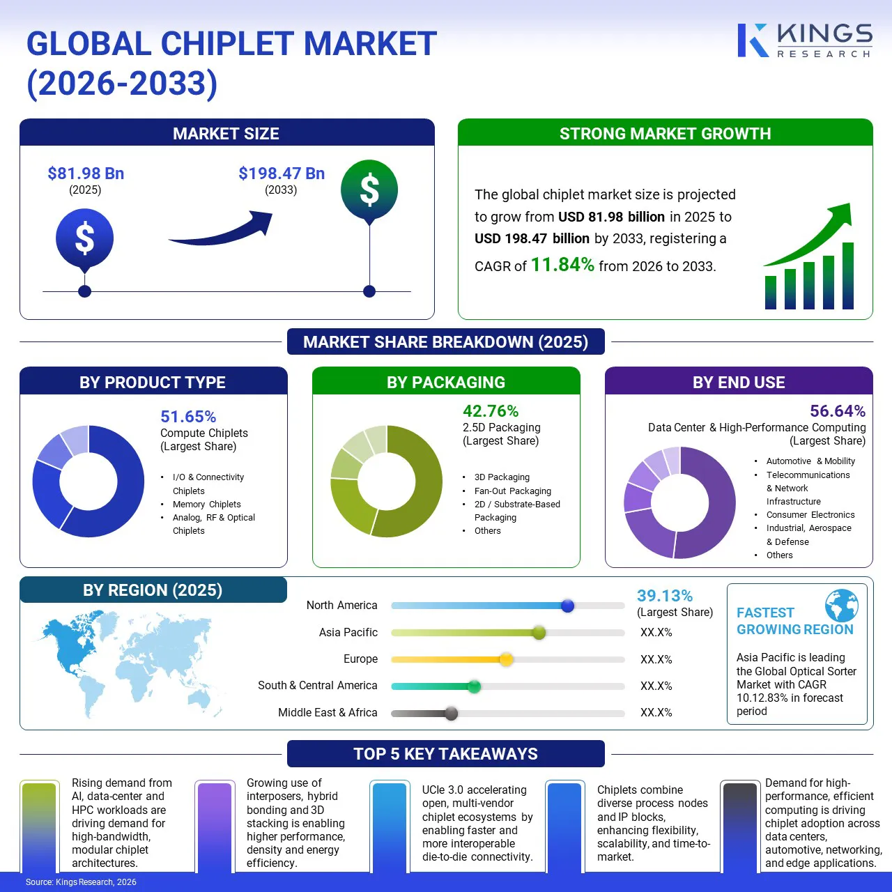
The global market is evolving from conventional monolithic chip architectures to modular and heterogeneous designs. This growth is fueled by the rising demand for high-performance and customized chips across data centers, artificial intelligence (AI), automotive, telecommunications, and industrial applications.
Chiplet and 3D IC technologies are increasingly viewed as key approaches to sustaining computing performance scaling, enabling the integration of multiple specialized chiplets within a single package to improve performance, power efficiency, and design flexibility. These capabilities are driving the adoption of high-density chiplet architectures for AI and high-performance computing applications, thereby boosting market growth.
Additionally, rising investments by leading semiconductor manufacturers, foundries, and packaging providers in advanced packaging, heterogeneous integration, and high-bandwidth memory (HBM) technologies are further strengthening the development and commercialization of chiplet-based solutions.
The flexibility and reusability of chiplets allow companies to build complex chips by combining smaller, separate components instead of designing an entire chip from scratch. This enables the reuse of existing chiplets, customization of products for different applications, improved performance, better power management, and reduced development time and associated costs.
Additionally, chiplets allow manufacturers to mix diverse node technologies within a single package, pairing cutting-edge, expensive process nodes for high-performance compute blocks with older, more cost-effective nodes for simpler functions. This flexibility accelerates the adoption of chiplets across high-growth domains, including data centers, artificial intelligence (AI), automotive systems, and industrial automation.
For instance, chiplets in automotive components reduce semiconductor costs by enabling smaller, specialized dies instead of large monolithic SoCs. This enables improved manufacturing yields and reusability of chiplet designs and thus facilitates the combination of different vehicle process technologies, including ADAS (Advanced Driver Assistance Systems), infotainment, EV powertrains, and associated control systems.
The high cost associated with chiplet production is attributed to additional manufacturing, testing, inspection, and advanced packaging costs. Chiplet production necessitates 2.5D and 3D advanced packaging methodologies, complex testing, and specialized inspection processes, which significantly increase upfront capital expenditures. Furthermore, capacity limitations among foundries and packaging service providers that handle chiplet-based designs limit scalability and hamper supply.
To address this challenge, market players are collaborating through open industry consortiums to establish standardized die-to-die interconnect protocols, such as Universal Chiplet Interconnect Express (UCIe). The standard sets guidelines for communications between chiplets, which encompass both protocols and physical connections. This enables different vendors to develop compatible chiplets, as manufacturers are able to utilize proven components from multiple sources instead of building everything from scratch.
Glass substrates enable dense chiplet arrangements by improving alignment, thermal stability, interconnect reliability, signal integrity, and overall manufacturing yield, compared to conventional substrates. Glass substrates with TGV (Through-Glass Via) technology, glass interposers, 2.5D/3D packaging, and heterogeneous integration position them as alternatives to organic substrates, ceramic substrates, and silicon interposers.
Additionally, the ability of glass substrates to reduce manufacturing defects and support miniaturization and high-performance semiconductor applications is creating new growth opportunities.
|
Segmentation |
Details |
|
|
By Product Type |
Compute Chiplets (Central Processing Unit (CPU), Graphics Processing Unit (GPU), AI/ML Accelerators & Neural Processing Units (NPUs), Field-Programmable Gate Arrays (FPGAs), Data Processing Units (DPUs) & SmartNIC Compute), I/O & Connectivity Chiplets (System I/O Controllers, Network & Communication PHYs, Die-to-Die Interconnect PHYs, CXL Memory Controllers & Expander Dies, Others), Memory Chiplets (HBM / Stacked Memory Dies, 3D Stacked Cache / SRAM, Others), Analog, RF & Optical Chiplets (PMICs & Voltage Regulators, Mixed-Signal & Data Converter Dies, RF & mmWave Transceiver Dies, Silicon Photonics & Co-Packaged Optical Engines, Others) |
|
|
By Packaging |
2.5D Packaging, 3D Packaging, Fan-Out Packaging, 2D / Substrate-Based Packaging, Others |
|
|
By End Use |
Data Center & High-Performance Computing (HPC), Automotive & Mobility, Telecommunications & Network Infrastructure, Consumer Electronics, Industrial, Aerospace & Defense, Healthcare & Medical Devices, Others |
|
|
By Region |
North America |
U.S., Canada, Mexico |
|
Europe |
France, UK, Spain, Germany, Italy, Russia, Rest of Europe |
|
|
Asia-Pacific |
China, Japan, India, Australia, ASEAN, South Korea, Rest of Asia-Pacific |
|
|
Middle East and Africa |
Turkey, U.A.E., Saudi Arabia, South Africa, Rest of Middle East & Africa |
|
|
South and Central America |
Brazil, Argentina, Rest of South and Central America |
|
The 3D packaging segment is poised to register the fastest growth rate of 17.93% over the forecast interval (2026-2033). This growth is attributed to the rising demand for higher bandwidth, improved power efficiency, and greater integration density. Its compact, high-performance architecture makes it well suited to advanced chiplet-based applications such as AI, HPC, and data centers.
The data centers and high-performance computing (HPC) segment accounted for a share of 56.64% in 2025. The high share is attributable to the rising adoption of chiplet-based architectures across artificial intelligence applications, data centers, and high-performance computing (HPC) systems, which enable scalable compute, higher bandwidth, and improved power efficiency.
The global chiplet industry is moderately consolidated, with leading semiconductor companies strengthening their competitive positions through strategic acquisitions and technology portfolio expansion. Merger and acquisition activities are focused on enhancing technological capabilities, expanding production capacity, and increasing market reach across emerging applications, including data centers and high-performance computing.
Based on region, the global market has been segmented into North America, Europe, Asia Pacific, the Middle East and Africa, and South and Central America.
North America captures the highest market share of 39.13% with a market valuation of USD 32.08 billion in 2025. The high share of the region is attributed to the presence of major semiconductor manufacturing and design ecosystems across the U.S.
In July 2025, semiconductor companies announced more than half a trillion dollars in private-sector investments to revitalize the U.S. chip ecosystem, aiming to set in motion a projected tripling of U.S. chip-making capacity by 2032.
Moreover, legislation passed in July 2025 to strengthen critical tax incentives, such as the Advanced Manufacturing Investment Credit (AMIC), further boosted investments from semiconductor companies. This is creating a favorable environment for regional market expansion.
Asia Pacific has emerged as the fastest-growing market, estimated to exhibit a CAGR of 12.83% over the forecast period (2026-2033). The growth is driven by the strong presence of semiconductor manufacturing facilities and increasing investments in advanced packaging technologies.
Countries including Taiwan, China, South Korea, and Japan account for a majority share in the global semiconductor manufacturing landscape. Market players such as Taiwan Semiconductor Manufacturing Company (TSMC), Samsung Electronics, and SK Hynix provide the essential wafer-level fabrication, 3D stacking, and high-bandwidth memory (HBM) integration required for modular chiplet designs.
Regional players are rapidly adopting advanced packaging solutions, with leading semiconductor manufacturers and packaging service providers supporting the integration of chiplets into high-performance computing and AI architectures.
The chiplet market is increasingly influenced by semiconductor manufacturing standards, safety requirements, government policies, and strategic initiatives aimed at strengthening advanced chip production. Regulatory developments across major chiplet manufacturing countries are supporting safer semiconductor manufacturing, while new policy measures are encouraging investment, innovation, and the development of resilient domestic chiplet and advanced-packaging ecosystems.
Capital deployment in the global chiplet market is increasingly focused on advanced packaging, heterogeneous integration, die-to-die interconnects, open chiplet standards, AI/HPC accelerators, and ecosystem development. Investment is also shifting toward building scalable manufacturing and packaging capacity as chiplet architectures become increasingly important for next-generation AI and high-performance computing.
Investment by leading foundries is increasingly targeting advanced packaging technologies required to integrate multiple chiplets into high-performance systems.
Investment and M&A activity is increasingly focused on acquiring critical chiplet IP, particularly high-speed die-to-die interconnect and analog/mixed-signal technologies.
Industry increasingly directs investment toward standardization and interoperability to reduce the complexity of integrating chiplets from multiple vendors.
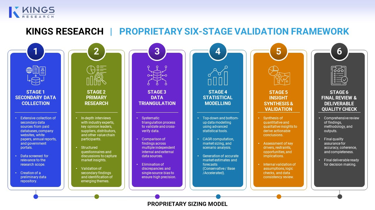
Our methodology triangulates insights from multiple independent and publicly available research databases, which is further validated against regulatory filings and public company disclosures. All estimates are cross-verified; no single-source data is presented without validation.
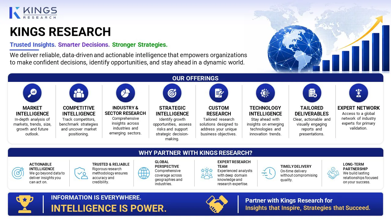
Our custom offerings deliver tailored, data-driven intelligence and strategic guidance to help organizations identify, evaluate, and capitalize on key market opportunities.
Frequently Asked Questions

Faizy brings over four years of experience in market research and consulting, with a proven ability to support strategic engagements across diverse industries and business environments. His work focuses on understanding complex market structures, identifying emerging opportunities, and translating research findings into clear, commercially relevant insights. With strong analytical capabilities and a structured approach to problem-solving, he evaluates industry trends, competitive landscapes, customer dynamics, and evolving business models. His expertise encompasses market research, competitive intelligence, market sizing and forecasting, industry assessment, company benchmarking, and strategic analysis. Faizy combines technical proficiency with a strong research orientation, enabling him to interpret both qualitative and quantitative information effectively. He has contributed to projects that help organizations assess growth potential, strengthen market positioning, and evaluate strategic priorities. His adaptable approach allows him to work across sectors while maintaining a consistent focus on accuracy, relevance, and delivering insights that support informed decision-making for clients and stakeholders.
Habi is a seasoned research and consulting leader with renowned experience in guiding clients on strategic growth and transformation initiatives across global markets. He has led high-performing research teams that deliver actionable insights on market expansion, M&A strategies, opportunity assessment, new business development, and product launches. His project portfolio spans large petrochemical producers, electronic device manufacturers, lubricants companies, and other leading enterprises across diverse industrial and consumer sectors. He currently heads the research department at Kings Research, where he is responsible for setting the research agenda, mentoring analysts, and ensuring client-ready deliverables that support executive decision-making. With extensive experience in market intelligence, strategic research, and consulting, Habi brings a strong understanding of evolving industry dynamics, competitive landscapes, emerging opportunities, and business growth challenges. His expertise includes developing research frameworks, translating complex market data into actionable strategic recommendations, and working closely with senior stakeholders to address critical business questions. He has also contributed to building research capabilities, strengthening analytical methodologies, and driving a culture of quality and insight-led decision-making within research teams. His cross-industry exposure enables him to connect market trends with broader business implications and provide perspectives that help organizations identify opportunities, mitigate risks, and make informed strategic decisions.