

As per Kings Research, the U.S. CoWoS market size was valued at USD 308.21 million in 2025 and is projected to reach USD 1,939.02 million by 2033, representing a CAGR of 26.10 percent over the forecast period. This rapid expansion highlights a massive shift in semiconductor manufacturing priorities. Artificial intelligence workloads demand massive computational power, pushing the limits of traditional silicon architectures. Advanced packaging solutions bridge the gap between processing capabilities and memory bandwidth, enabling faster data transfer speeds.
For industry professionals tracking semiconductor supply chain resilience, understanding advanced packaging dynamics is essential. The U.S. is actively exploring pathways to build domestic capacity, reduce offshore dependencies, and foster an independent semiconductor ecosystem. This analysis explores capacity constraints, government investments, alternative hardware architectures, and the strategic positioning required for the U.S. to compete globally.
What Is CoWoS?
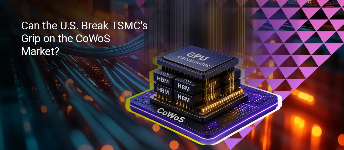
Chip on Wafer on Substrate (CoWoS) is an advanced packaging methodology crafted by TSMC. It lets hardware developers place multiple active dies like Graphics Processing Units and High Bandwidth Memory side by side on a single platform.
This base, called a silicon interposer, acts as a high-speed bridge. Rather than placing chips directly on a standard circuit board, builders mount them on this interposer. The interposer features thousands of microscopic wires that link the chips together. This microscopic proximity allows data to travel at extreme speeds with very little latency. After the chips are securely attached to the interposer, this entire assembly is attached to a larger organic substrate. This final layer links the dense micro components to the broader server architecture.
Why is this methodology critical? Legacy architectures struggle with a bottleneck where the processor waits for data to arrive from separate memory chips. By utilizing this 2.5D integration, data transfer happens seamlessly.
Why Is TSMC's Dominance Central to the U.S. CoWoS Market?
Taiwan Semiconductor Manufacturing Company (TSMC) established early leadership in advanced packaging through years of continuous research and development. By integrating wafer fabrication with sophisticated packaging techniques, the firm created a seamless, end-to-end manufacturing process. This integration ensures high yields, superior performance, and reliable delivery schedules for the world's leading fabless semiconductor designers. The concentration of packaging capabilities creates vulnerabilities for the U.S. semiconductor supply chain. TSMC's early investments allowed the firm to refine the Chip on Wafer on Substrate process long before competitors realized the impending demand surge driven by artificial intelligence. Today, major U.S. firms rely heavily on this centralized capacity.
To address these vulnerabilities, the U.S. government enacted the CHIPS and Science Act, which provides USD 50 billion to the Department of Commerce, with USD 39 billion dedicated directly to funding incentives for domestic semiconductor facilities and equipment, including advanced packaging (Note that CHIPS funding figures are nested, not additive: the USD 50 billion fund contains the USD 39 billion incentives program and the USD 11 billion R&D allocation, which in turn houses the NAPMP's approximately USD 3 billion and its specific awards). This massive capital injection aims to mitigate the risks associated with overseas reliance and bring manufacturing control back to domestic soil.
What Makes CoWoS the Most Critical Bottleneck in the AI Chip Supply Chain?
Artificial intelligence infrastructure relies entirely on the seamless flow of data between processing units and memory. The Chip on Wafer on Substrate process provides the essential physical bridge connecting GPUs with High Bandwidth Memory. Without this advanced packaging step, individual high-performance chips remain isolated and fail to process complex AI algorithms efficiently.
The current supply chain experiences severe oversubscription dynamics. Fabless semiconductor companies place orders years in advance, securing packaging capacity to guarantee future product releases. This long-term booking strategy leaves smaller players struggling to secure allocations. As highlighted in our comprehensive U.S. CoWoS Market Report, lead times for advanced packaging can stretch considerably, frequently delaying the deployment of critical data center infrastructure. The precision required for placing microscopic bumps on silicon interposers demands specialized equipment and highly controlled cleanroom environments, making rapid expansion incredibly difficult.
How Is AI Infrastructure Demand Influencing the U.S. CoWoS Market?
Data centers are undergoing a massive evolution to support generative AI training workloads. Traditional cloud computing infrastructure relied on general-purpose processors, whereas modern AI applications require dense clusters of specialized accelerators. These GPU clusters demand extraordinary memory bandwidth to process trillions of parameters simultaneously. Hyperscalers are deploying capital at unprecedented rates to secure hardware capable of training next-generation large language models. The U.S. houses the largest concentration of these cloud service providers, driving immense domestic demand for packaged AI chips.
Recognizing this massive demand, the U.S. government established the National Advanced Packaging Manufacturing Program, allocating approximately USD 3 billion in funding, as detailed in a November 2023 NIST release, to drive U.S. leadership specifically in advanced packaging capabilities. This initiative directly addresses the infrastructure requirements of modern AI data centers by accelerating domestic manufacturing scale and ensuring stable hardware availability for the world's largest cloud providers.
Why Does Capacity Concentration Outside the U.S. Limit Domestic Growth?
The vast majority of advanced packaging facilities are located in Asia, creating a geographic disconnect between chip designers in Silicon Valley and their manufacturing partners overseas. This physical distance introduces logistical complexities, intellectual property risks, and vulnerability to geopolitical tensions. Relying on offshore packaging facilities limits the agility of U.S. semiconductor firms. Rapid prototyping and iterative testing become cumbersome when hardware must cross the Pacific Ocean multiple times during the manufacturing cycle. Domestic growth is constrained by the inability to quickly scale production in response to sudden market shifts.
The U.S. semiconductor industry loses valuable learning cycles when manufacturing occurs elsewhere. Engineers working directly on the factory floor discover incremental process improvements that compound over time. By outsourcing the packaging step, the U.S. misses out on these critical optimization opportunities, gradually eroding domestic technical expertise. Rebuilding this capability requires restoring the physical proximity between research, design, and manufacturing teams.
What Role Do U.S. Investments and Policies Play in Reducing Dependency?
Federal incentives serve as the primary catalyst for expanding the domestic packaging ecosystem. The U.S. government understands that securing a robust semiconductor supply chain requires financial intervention to offset the high costs of building local facilities. These targeted public funds have successfully mobilized massive private capital.
The U.S. Department of Commerce stated that the CHIPS National Advanced Packaging Manufacturing Program finalized USD 1.4 billion in award funding to bolster U.S. leadership in advanced packaging. In August 2025, the Commerce Department voided its January 2025 agreement with Natcast, which included a $1.1 billion advanced-packaging award, and transferred operational responsibility for the NSTC to NIST. The status of the Tempe, Arizona piloting facility remains unresolved. These investments aim to create a self-sustaining ecosystem where advanced chips are both manufactured and packaged within the U.S. By lowering the financial barriers to entry, the government empowers domestic firms to develop competing techniques, build modern facilities, and train a specialized workforce capable of challenging established overseas dominance.
Can Emerging Packaging Alternatives Challenge CoWoS Dominance?
While TSMC leads the 2.5D packaging sector, competing architectures are emerging to address cost and scalability concerns. Chipmakers are exploring alternative methodologies to bypass current supply constraints and offer differentiated products to hyperscalers. Intel introduced the Embedded Multi die Interconnect Bridge (EMIB) to challenge existing packaging paradigms. Instead of using a large, expensive silicon interposer, EMIB uses small silicon bridges embedded directly into the organic substrate to connect adjacent chiplets. This approach reduces costs and improves manufacturing yields for large area packages.
Panel Level Packaging (PLP) offers a highly promising alternative. Traditional methods process circular silicon wafers, leaving wasted space at the edges. Panel Level Packaging processes rectangular panels, significantly increasing the usable area and reducing the cost per package.
Advanced Packaging Architecture Comparison
|
Architecture |
Provider |
Key Advantage |
Limitation |
Use Case |
|
CoWoS |
TSMC |
Proven reliability, ultra-high interconnect density |
High cost, severe capacity constraints |
Flagship AI accelerators, Data center GPUs |
|
EMIB |
Intel |
Lower cost, localized high-density routing |
Complex substrate manufacturing requirements |
High performance computing, FPGA integration |
|
Panel Level Packaging (PLP) |
Samsung / Powertech / SPIL / ASE |
Higher area utilization, reduced unit cost |
Immature equipment ecosystem, yield challenges |
Consumer electronics, automotive chips |
|
FOPLP |
ASE (310mm) / Amkor (650mm) |
Flexible integration, strong supply chain diversity |
Lower maximum interconnect density |
Networking chips, mid-tier AI processors |
Source: Industry analyses and manufacturer specifications.
How Are Strategic Partnerships Shaping the Competitive Landscape?
Single firms rarely possess the resources to build a comprehensive domestic packaging ecosystem independently. Strategic alliances are forming across the industry to share costs, pool technical expertise, and accelerate the deployment of new facilities. A prominent example is the collaboration between TSMC and Amkor. These two giants formed a 10-year partnership to expand packaging capabilities in Arizona, establishing a critical center for advanced packaging within the domestic supply chain.
Public and private collaborations also drive significant capital injection into the sector. For instance, up to USD 300 million in federal funding will be paired with additional investments from the private sector, bringing the expected total investment across key advanced substrate research projects in states like Georgia, California, and Arizona to over USD 470 million. This collaborative framework is essential for establishing long-term engineering leadership and securing the domestic supply chain against future disruptions.
What Financial Barriers Prevent Rapid U.S. Expansion in CoWoS?
Building advanced packaging facilities requires staggering capital expenditures. A modern plant costs billions of dollars to construct and equip. The specialized machinery required for wafer bumping, interposer attachment, and precision metrology commands premium prices and suffers from long delivery lead times. Operating these facilities in the U.S. introduces higher baseline costs compared to Asian locations. Labor, utilities, and regulatory compliance all contribute to a steeper operational curve. These elevated expenses force U.S. facilities to target high-margin products, leaving lower-tier packaging segments vulnerable to overseas competition.
Skilled workforce limitations represent a formidable barrier. Advanced packaging requires engineers with deep expertise in materials science, fluid dynamics, and thermomechanical stress analysis. The U.S. education system is currently ramping up programs to train this specialized workforce, but the talent pipeline requires years to mature. Supply chain limitations also hinder rapid expansion, as the chemical precursors, specialized substrates, and cleanroom consumables required for packaging are frequently sourced from international vendors.
How Do Hyperscalers Influence Power Dynamics in the CoWoS Market?
Cloud service providers and large enterprise buyers wield immense influence over the semiconductor supply chain. Companies designing flagship GPUs dictate the technical specifications and volume requirements that manufacturers must meet. The sheer scale of their purchasing power shapes the strategic direction of packaging providers. Large buyers secure their supply through massive upfront payments and long-term capacity reservations. These financial commitments provide manufacturers with the capital required to expand their facilities.
The federal government recognizes the influence of these market dynamics. In response, a portion of the USD 50 billion CHIPS Act is specifically utilized to ensure broader market access; the Department of Commerce designated USD 11 billion of this total for establishing a robust domestic semiconductor research and development ecosystem. This ensures that smaller semiconductor startups can access the research and packaging resources needed to launch competing products, preventing hyperscalers from entirely dominating future domestic packaging capacity.
Ready to dive deeper into supply chain dynamics? Download our full semiconductor sector report to access comprehensive data and strategic forecasts.
What Future Scenarios Could Shift the Balance in the U.S. CoWoS Market?
The trajectory of the advanced packaging sector remains highly dynamic. As previously stated, the U.S. CoWoS market is projected to reach USD 1,939.02 million by 2033, creating a massive financial incentive for domestic firms to capture value. Several potential scenarios could define the coming decade.
Scenario 1: Continued TSMC Dominance
Despite massive U.S. investments, TSMC maintains its overwhelming lead by continuously executing flawless generation transitions and expanding its CoWoS capacity globally. U.S. facilities serve primarily as backup sites or niche production centers, while the bulk of high-volume AI chip packaging remains concentrated overseas.
Scenario 2: Partial U.S. Independence
Federal funding and private partnerships successfully establish a robust, secondary packaging ecosystem within the U.S. Major AI hardware companies dual-source their packaging needs, splitting volume between offshore facilities and newly constructed domestic plants. This scenario significantly improves supply chain resilience and mitigates geopolitical risks.
Scenario 3: Architectural Disruption
Alternative packaging techniques, such as glass substrates or Panel Level Packaging, mature faster than anticipated. U.S. based companies pioneer these breakthroughs, rendering traditional silicon interposer methods obsolete for certain applications. This paradigm shift allows domestic manufacturers to leapfrog established players and capture a significant share of the advanced packaging sector.
Looking for deeper data and market forecasts?
Access the comprehensive strategic research report covering domestic advanced packaging growth.
View the U.S. CoWoS Market Report | Kings Research
FAQs
Why is CoWoS capacity limited?
Capacity remains constrained due to the extreme complexity of the manufacturing process, shortages of specialized packaging equipment, and unprecedented demand from AI hardware developers securing long term reservations.
Can the U.S. build its own CoWoS ecosystem?
The U.S. is actively building domestic capabilities through massive federal investments, strategic partnerships, and focused research initiatives, aiming to create a self-sustaining packaging infrastructure.
What companies dominate CoWoS packaging?
TSMC holds the dominant position in manufacturing and packaging, while fabless designers and major cloud service providers drive the primary demand for these advanced components.
How does CoWoS impact AI chip production?
It serves as the critical physical bridge connecting processing units with High Bandwidth Memory, directly determining the data transfer speeds and overall performance of AI hardware.
What alternatives exist to CoWoS?
Industry alternatives include Intel's EMIB architecture, Panel Level Packaging (PLP), and advanced organic substrates, all designed to offer varying balances of cost, density, and scalability.