
Inquire Now
Key Strategic Points
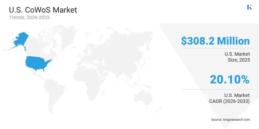
According to Kings Research, the U.S. CoWoS market size was valued at USD 308.21 million in 2025 and is projected to reach USD 1,939.02 million by 2033, growing at a CAGR of 26.10% from 2026 to 2033. The market is driven by increasing demand for advanced semiconductor packaging capable of integrating multiple processors, high-bandwidth memory (HBM) stacks, and memory dies within a single high-performance package.
The CoWoS (Chip-on-Wafer-on-Substrate) technology enables heterogeneous integration of logic processors, GPUs, AI accelerators, SoCs, chiplets, and HBM into a single package. The technology addresses the increasing computational and memory-bandwidth requirements of artificial intelligence (AI), high-performance computing (HPC), and data-center applications. Rising investments in advanced packaging technologies, semiconductor fabrication capacity, and next-generation processors are creating further opportunities for the U.S. CoWoS market.
Key companies operating in the market, including Taiwan Semiconductor Manufacturing Company, Samsung Electronics, ASE Technology Holding, Amkor Technology, Intel Corporation, NVIDIA, AMD, Broadcom, Deca Technologies, Micron Technology, Powertech Technology, and others, are expanding production and advanced packaging capabilities to address increasing demand for AI and high-performance computing applications.
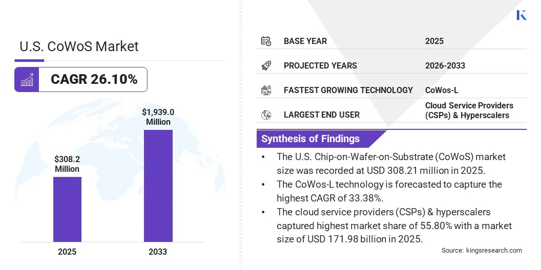
Increasing demand for AI, machine learning, and data-center applications is driving the adoption of advanced semiconductor packaging technologies such as CoWoS. The technology enables GPUs and AI accelerators to be integrated with HBM on a common substrate, improving memory bandwidth and processing performance for demanding workloads.
The U.S.'s strong data-center and HPC ecosystem is further supporting demand for high-performance processors.
The concentration of advanced CoWoS packaging capacity represents a major constraint for the U.S. market. Rising demand from AI chip manufacturers has placed substantial pressure on existing capacity, while limited production availability and long lead times can restrict the supply of advanced packaged chips.
TSMC's dominant position in CoWoS manufacturing creates additional supply-chain concentration. In December 2025, its CoWoS-S and CoWoS-L lines were reportedly fully booked, with lead times ranging from 52 to 78 weeks. NVIDIA, Broadcom, and AMD together accounted for more than 85% of TSMC's CoWoS capacity, further highlighting the concentration of demand.
To address these constraints, semiconductor companies are investing in alternative advanced packaging technologies and domestic production capabilities. In March 2026, Intel moved its EMIB-T advanced packaging technology into production, targeting greater diversification in the advanced packaging ecosystem.
Panel-Level Packaging (PLP) is emerging as a potential alternative to conventional wafer-based packaging by using larger rectangular panels to improve manufacturing efficiency, throughput, and cost economics. The technology can support larger packages and the high-density interconnects required for AI accelerators and HPC applications.
Chip-on-Panel-on-Substrate (CoPoS) is another emerging technology that replaces conventional silicon interposers with glass-based substrates, enabling larger AI chip packages.
|
Segmentation |
Details |
|
By Technology |
CoWos-S, CoWos-R, CoWos-L |
|
By Component Type |
ASIC, CPU, FPGA, GPU, Others |
|
By End User |
Cloud Service Providers (CSPs) & Hyperscalers, AI Cloud & GPU-as-a-Service Providers, Enterprise Data Centers, Telecommunications & Networking, Government, Defense & Supercomputing Centers, Others |
Based on technology, the market is categorized into CoWoS-S, CoWoS-R, and CoWoS-L. CoWoS-L is expected to register the highest CAGR of 33.38% over the forecast period as AI accelerators and HPC processors require increasingly large package sizes, higher interconnect density, and advanced multi-chip integration.
The technology combines the advantages of CoWoS architecture with advanced interconnect capabilities, making it suitable for next-generation AI processors and high-performance computing applications. The increasing complexity of AI accelerator architectures is expected to support demand for CoWoS-L technology.
Based on component type, the market is classified into ASIC, CPU, FPGA, GPU, and Others. ASICs represented the largest component segment of 63.40% in 2025, supported by their increasing deployment in AI accelerators and specialized computing systems.
ASICs benefit from application-specific architectures that can provide high performance and power efficiency for targeted workloads. As AI infrastructure expands, demand for specialized accelerators is increasing, supporting the use of CoWoS packaging for high-performance ASIC designs.
GPUs also represent a significant opportunity as they remain widely deployed across AI training, inference, cloud computing, and HPC applications.
Based on end user, the market is segmented into Cloud Service Providers (CSPs) & Hyperscalers, AI Cloud & GPU-as-a-Service Providers, Enterprise Data Centers, Telecommunications & Networking, Government, Defense & Supercomputing Centers, and Others.
Cloud service providers and hyperscalers accounted for the largest share of 55.80% in 2025. Their leading position is supported by rapid expansion of AI infrastructure, hyperscale data centers, and cloud-based computing services.
The increasing deployment of GPUs and AI accelerators for model training and inference requires advanced packaging solutions that deliver high memory bandwidth and processing performance. Continued investment in AI-focused data centers is therefore expected to support CoWoS demand among hyperscale operators.
The dominance of the U.S. in data centers, artificial intelligence, and high-performance computing fuels the demand for logic chips required to train, deploy, and enhance the computational power of AI models. The rise in demand is driving investments in the U.S. semiconductor industry to increase chip production, with the CHIPS and Science Act acting as a pivotal base boosting new private investments in semiconductor manufacturing estimated at USD 450 billion across 28 states in the U.S. The demand for efficient chips that combine multiple dies and pack on a single substrate and offer improved power efficiency, thermal performance, and a compact footprint critical for AI, HPC, and cloud workloads drives the growth of the CoWoS market in the U.S.
Additionally, advanced LLMs and increasing generative AI applicability across the commercial and industrial landscape of the U.S. further fuel high-capacity and fast memory processing chips that handle the rising computing workloads. The transition of artificial intelligence beyond pilot projects towards embedding AI directly into core business operations further drives the demand for efficient computing chips, thereby creating growth avenues for CoWoS in the U.S. market.
Key players operating in the market are incorporating strategic mergers, acquisitions, and technical collaborations to strengthen their competitive positioning and capture a larger share of the market. Market players are emphasizing expansion of advanced packaging capacity, strengthening supply chain capabilities, and securing long-term manufacturing partnerships to address the rising demand for AI and high-performance computing applications. Companies are further undertaking strategic acquisitions to accelerate capacity expansion and gain access to advanced production infrastructure and investing in next-generation packaging technologies to cater to future demands for AI chips.
How We Gather This Information
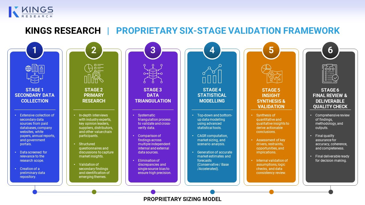
Our methodology triangulates insights from multiple independent and publicly available research databases and is further validated against regulatory filings and public company disclosures. All estimates are cross-verified; no single-source data is presented without validation.
 Why Kings Research?
Our custom offerings deliver tailored, data-driven intelligence and strategic guidance to help organizations identify, evaluate, and capitalize on key market opportunities.
Frequently Asked Questions

Faizy brings over four years of experience in market research and consulting, with a proven ability to support strategic engagements across diverse industries and business environments. His work focuses on understanding complex market structures, identifying emerging opportunities, and translating research findings into clear, commercially relevant insights. With strong analytical capabilities and a structured approach to problem-solving, he evaluates industry trends, competitive landscapes, customer dynamics, and evolving business models. His expertise encompasses market research, competitive intelligence, market sizing and forecasting, industry assessment, company benchmarking, and strategic analysis. Faizy combines technical proficiency with a strong research orientation, enabling him to interpret both qualitative and quantitative information effectively. He has contributed to projects that help organizations assess growth potential, strengthen market positioning, and evaluate strategic priorities. His adaptable approach allows him to work across sectors while maintaining a consistent focus on accuracy, relevance, and delivering insights that support informed decision-making for clients and stakeholders.
Habi is a seasoned research and consulting leader with renowned experience in guiding clients on strategic growth and transformation initiatives across global markets. He has led high-performing research teams that deliver actionable insights on market expansion, M&A strategies, opportunity assessment, new business development, and product launches. His project portfolio spans large petrochemical producers, electronic device manufacturers, lubricants companies, and other leading enterprises across diverse industrial and consumer sectors. He currently heads the research department at Kings Research, where he is responsible for setting the research agenda, mentoring analysts, and ensuring client-ready deliverables that support executive decision-making. With extensive experience in market intelligence, strategic research, and consulting, Habi brings a strong understanding of evolving industry dynamics, competitive landscapes, emerging opportunities, and business growth challenges. His expertise includes developing research frameworks, translating complex market data into actionable strategic recommendations, and working closely with senior stakeholders to address critical business questions. He has also contributed to building research capabilities, strengthening analytical methodologies, and driving a culture of quality and insight-led decision-making within research teams. His cross-industry exposure enables him to connect market trends with broader business implications and provide perspectives that help organizations identify opportunities, mitigate risks, and make informed strategic decisions.