Market Definition
The market includes tools and systems used in producing semiconductor devices through processes such as lithography, etching, deposition, ion implantation, and cleaning. These machines enable the creation of integrated circuits with nanometer-scale precision.
The market includes front-end equipment for wafer processing and back-end tools for assembly and testing. It supports the fabrication of microprocessors, memory chips, and logic devices used in electronics, automotive systems, data centers, and communications.
The report provides a comprehensive analysis of key drivers, emerging trends, and the competitive landscape expected to influence the market over the forecast period.
Semiconductor Manufacturing Equipment Market Overview
The global semiconductor manufacturing equipment market size was valued at USD 107.71 billion in 2024 and is projected to grow from USD 118.86 billion in 2025 to USD 248.48 billion by 2032, exhibiting a CAGR of 11.11% during the forecast period.
Market growth is driven by OEM investments in capacity expansion and in-house chip production to strengthen supply chain control. Additionally, innovations in semiconductor design are increasing the demand for advanced equipment capable of supporting complex architectures and precision manufacturing at smaller process nodes.
Major companies operating in the semiconductor manufacturing equipment industry are ADVANTEST CORPORATION, Hitachi, Ltd., Plasma-Therm, ASM International N.V., EV Group (EVG), Onto Innovation, Nikon Corporation, SENTECH Instruments GmbH, Applied Materials, Inc., ASML, Tokyo Electron Limited, SCREEN Semiconductor Solutions Co., Ltd, Nordson Corporation, Modutek Corporation, and Ferrotec Corporation.
The growth of market is significantly influenced by the increasing demand for high-performance consumer electronics. Devices such as smartphones, laptops, wearables, and smart appliances rely on powerful chips.
Manufacturers are expanding production capabilities to meet rising demand for speed, storage, and efficiency. This highlights the urgent need for more precise and scalable semiconductor equipment, fueling market growth across multiple regions prioritizing consumer electronics manufacturing.
- In March 2025, Hitachi High-Tech Corporation commenced operations at its new production facility dedicated to semiconductor manufacturing equipment, focused on etch systems. The facility increases production capacity by incorporating digitalized and automated manufacturing lines.

Key Highlights
- The semiconductor manufacturing equipment market size was valued at USD 107.71 billion in 2024.
- The market is projected to grow at a CAGR of 11.11% from 2025 to 2032.
- Asia Pacific held a market share of 68.42% in 2024, with a valuation of USD 73.70 billion.
- The front-end equipment segment garnered USD 79.18 billion in revenue in 2024.
- The 2D segment is expected to reach USD 136.96 billion by 2032.
- The semiconductor fabrication plant/foundry segment secured the largest revenue share of 46.53% in 2024.
- Europe is anticipated to grow at a CAGR of 11.59% over the forecast period.
Market Driver
OEM Investment in Capacity Expansion and In-House Chip Production
Original equipment manufacturers across sectors such as automotive, consumer electronics, and industrial automation are increasing investments in semiconductor capabilities to reduce supply chain risks and gain more control over product performance. This includes setting up captive fabs or partnering with foundries to secure dedicated production lines.
These efforts are fueling the growth of market, as OEMs require advanced lithography, inspection, and testing tools to support proprietary chip designs and ensure consistent production quality.
- The Semiconductor Equipment and Materials International (SEMI) reported in December 2024 that global sales of total semiconductor manufacturing equipment by original equipment manufacturers (OEMs) reached USD 113 billion, marking a 6.5% year-on-year increase and setting a new record for the industry. The global sales of the semiconductor manufacturing equipment are expected to reach USD 121 billion in 2025 and USD 139 billion in 2026, maintaining a strong upward trajectory.
Market Challenge
High Cost and Complexity of Advanced Equipment
A significant challenge affecting the growth of the semiconductor manufacturing equipment market is the high cost and technical complexity of next-generation tools. Equipment for advanced nodes, EUV lithography, and 3D packaging requires substantial capital investment and specialized knowledge, which limits access for smaller players and slows production scaling.
To address this challenge, key players are increasing collaboration through joint ventures and technology alliances. Many are also investing in modular and scalable equipment platforms to reduce initial costs. Additionally, some firms are expanding training and support services to help customers manage complex installations and improve long-term efficiency.
Market Trend
Innovations in Semiconductor Design
Advancements in chip architecture, including smaller nodes and 3D integration, are emerging as a notable trend in the market. Complex fabrication processes require highly specialized tools for patterning, deposition, and inspection.
The transition to FinFET and gate-all-around further boosts the demand for next-generation equipment. Foundries and integrated device manufacturers are upgrading their production lines, aiding the sales of advanced tools that support high-density, low-power chip manufacturing.
- In April 2025, Japan's New Energy and Industrial Technology Development Organization (NEDO) approved Rapidus Corporation's fiscal year 2025 plan and budget for 2nm semiconductor projects. The initiative includes the development of redistribution layer interposer technology, 3D packaging techniques, and assembly design kits, with equipment installation at the RCS site.
Semiconductor Manufacturing Equipment Market Report Snapshot
|
Segmentation
|
Details
|
|
By Equipment Type
|
Front-end Equipment (Silicon Wafer Manufacturing, Wafer Processing Equipment), Back-end Equipment (Testing Equipment, Assembling & Packaging Equipment)
|
|
By Dimension
|
2D, 2.5D, 3D
|
|
By Application
|
Semiconductor Fabrication Plant/Foundry, Semiconductor Electronics Manufacturing, Test Home
|
|
By Region
|
North America: U.S., Canada, Mexico
|
|
Europe: France, UK, Spain, Germany, Italy, Russia, Rest of Europe
|
|
Asia-Pacific: China, Japan, India, Australia, ASEAN, South Korea, Rest of Asia-Pacific
|
|
Middle East & Africa: Turkey, U.A.E., Saudi Arabia, South Africa, Rest of Middle East & Africa
|
|
South America: Brazil, Argentina, Rest of South America
|
Market Segmentation
- By Equipment Type (Front-end Equipment and Back-end Equipment): The front-end equipment segment earned USD 79.18 billion in 2024 due to its critical role in wafer fabrication processes, which requires high capital expenditure and advanced precision tools to support shrinking node sizes and complex chip architectures.
- By Dimension (2D, 2.5D, and 3D): The 2D segment held a share of 56.71% in 2024, attributed to its widespread adoption in high-volume production.
- By Application (Semiconductor Fabrication Plant/Foundry, Semiconductor Electronics Manufacturing, and Test Home): The semiconductor fabrication plant/foundry segment is projected to reach USD 119.79 billion by 2032, owing to continuous investments in advanced node production and high-volume chip manufacturing.
Semiconductor Manufacturing Equipment Market Regional Analysis
Based on region, the global market has been classified into North America, Europe, Asia Pacific, Middle East & Africa, and South America.
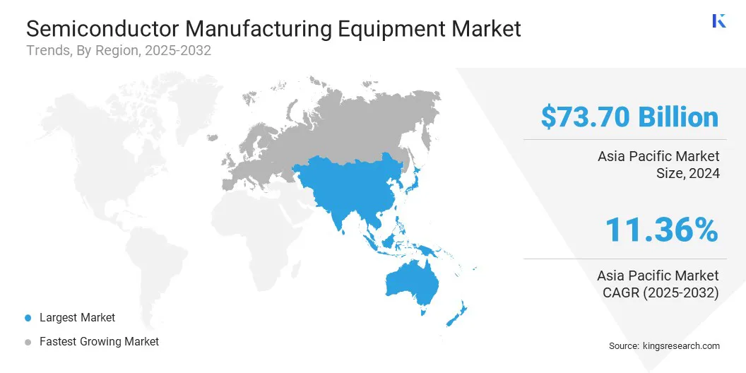
The Asia Pacific semiconductor manufacturing equipment market share stood at around 68.42% in 2024, valued at USD 73.70 billion. Asia Pacific is home to some of the world’s largest contract semiconductor foundries, which continue to expand production capacity to meet rising demand.
These foundries consistently invest in advanced lithography, etching, and deposition tools to manufacture high-performance chips for global clients, aiding regional market growth. Moreover, the region's extensive network of electronics manufacturers, including OEMs, ODMs, and EMS providers, ensures strong integration with semiconductor suppliers, sustaining demand for advanced fabrication equipment.
- In April 2025, United Microelectronics Corporation (UMC) inaugurated a new semiconductor fabrication facility in Singapore's Pasir Ris Wafer Fab Park. The first phase of this greenfield expansion involves an investment of up to USD 5 billion to achieve a production capacity of 30,000 wafers per month, with provisions for further expansion.
The Europe semiconductor manufacturing equipment industry is estimated to grow at a CAGR of 11.59% over the forecast period. Europe’s research institutions and semiconductor R&D centers are involved in developing new materials, lithography techniques, and chip architectures. These innovation hubs often partner with equipment manufacturers for prototype development and testing, contributing to market expansion.
- In May 2025, Thales, Radiall, and Foxconn initiated discussions to establish a semiconductor assembly and test facility in France. The proposed plant aims to produce over 100 million system-in-package units annually by 2031, with an investment exceeding USD 273 million. This initiative seeks to bolster Europe's semiconductor manufacturing capabilities and technological capacity.
Furthermore, Europe is directing public and private investment toward strategic semiconductor initiatives aimed at strengthening the region’s production capabilities. These projects include new fabrication plants, pilot lines, and advanced packaging facilities, particularly in support of industrial and automotive applications, which is bolstering regional market expansion.
- In February 2025, the European Commission approved approximately USD 1 billion state aid package from Germany to Infineon for constructing the MEGAFAB-DD semiconductor manufacturing facility in Dresden. This project is part of the broader European Chips Act, focusing on enhancing Europe's semiconductor production capacity and supply security. The facility is expected to reach full capacity by 2031, producing diverse chips for industrial, automotive, and consumer applications.
Regulatory Frameworks
- In the U.S., semiconductor manufacturing equipment is regulated under the Export Administration Regulations (EAR) by the Bureau of Industry and Security (BIS), which oversees exports to protect national security and prevent technology transfer to restricted entities. The Environmental Protection Agency (EPA) enforces strict standards on emissions, chemical handling, and waste disposal standards for fabs and suppliers. Further, compliance with workplace safety is regulated by OSHA standards.
- The semiconductor manufacturing equipment industry in Europe is regulated by the EU’s REACH (Registration, Evaluation, Authorization and Restriction of Chemicals) regulation. It imposes strict controls on hazardous substances used in manufacturing processes and equipment. The Waste Electrical and Electronic Equipment Directive (WEEE) also governs disposal and recycling obligations. Trade and dual-use export controls come under the EU Dual-Use Regulation, which aligns with international non-proliferation efforts
- China regulates semiconductor manufacturing equipment under strict export controls administered by the Ministry of Commerce (MOFCOM). Recently tightened controls focus on limiting advanced semiconductor technology exports to maintain domestic industry leadership and address security concerns. Environmental regulations from the Ministry of Ecology and Environment (MEE) control emissions and hazardous waste during manufacturing.
- Japan oversees semiconductor equipment manufacturing through export controls managed by the Ministry of Economy, Trade and Industry (METI), focusing on dual-use technologies to prevent misuse. Environmental regulations under the Basic Environment Law and the Chemical Substances Control Law impose strict standards on chemical usage and emissions. The country also enforces workplace safety standards specific to manufacturing under the Industrial Safety and Health Act.
Competitive Landscape
Major players in the semiconductor manufacturing equipment market are forming strategic partnerships, investing in advanced technology, and expanding manufacturing capabilities. These approaches enable companies to strengthen their product offerings and improve infrastructure.
- In September 2024, Tata Electronics signed a memorandum of understanding with Tokyo Electron Limited (TEL), a global provider of semiconductor equipment and services. The partnership aims to fast-track the development of semiconductor equipment infrastructure for Tata Electronics’ first fabrication plant in Gujarat, as well as its assembly and testing facility in Assam. This collaboration is expected to combine the expertise of both companies to build a strong semiconductor manufacturing ecosystem in India.
List of Key Companies in Semiconductor Manufacturing Equipment Market:
- ADVANTEST CORPORATION
- Hitachi, Ltd.
- Plasma-Therm
- ASM International N.V.
- EV Group (EVG)
- Onto Innovation
- Nikon Corporation
- SENTECH Instruments GmbH
- Applied Materials, Inc.
- ASML
- Tokyo Electron Limited
- SCREEN Semiconductor Solutions Co., Ltd
- Nordson Corporation
- Modutek Corporation
- Ferrotec Corporation
Recent Developments (Expansion/Product Launch)
- In May 2025, GlobalWafers opened a USD 3.5 billion advanced 300-mm wafer facility in Sherman, Texas, in over 20 years. This facility aims to meet the increasing demand from U.S. customers for locally produced wafers and is part of the CHIPS for America program.
- In March 2025, EV Group (EVG) introduced the next-generation GEMINI automated production wafer bonding system for 300-mm wafers. Built on the globally recognized standard for high-volume wafer bonding, the updated GEMINI platform features a newly engineered high-force bond chamber designed to deliver superior bond quality and yield, particularly for MEMS devices manufactured on larger wafers.
- In October 2024, KLA Corporation launched the industry's most comprehensive range of process control and process-enabling solutions for IC substrate (ICS) manufacturing. Leveraging its expertise in front-end semiconductors, packaging, and IC substrates, KLA aims to advance packaging interconnect density for chips for high-performance applications.


