Market Definition
Atomic layer deposition (ALD) is a precise thin-film deposition technique that provides atomic-level control over material coatings. This process operates through sequential, self-limiting chemical reactions, ensuring uniformity and high quality on both flat and complex 3D surfaces. It is widely used in semiconductors, energy devices, nanotechnology, and advanced coatings due to its accuracy and ability to produce ultra-thin, defect-free films.
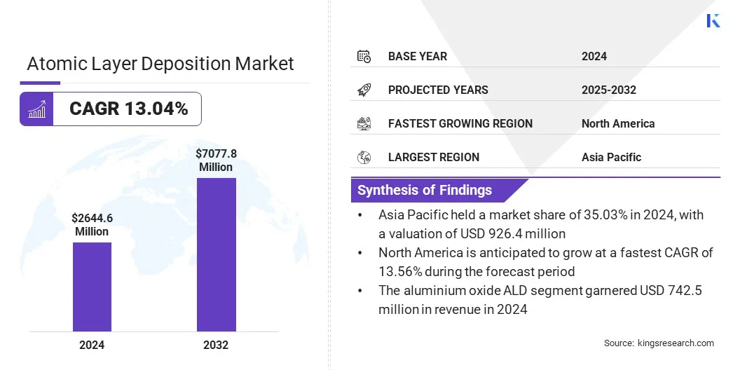
Atomic Layer Deposition Market Overview
The global atomic layer deposition market size was valued at USD 2,644.6 million in 2024 and is projected to grow from USD 2,982.6 million in 2025 to USD 7,077.8 million by 2032, exhibiting a CAGR of 13.04% during the forecast period.
Rising demand for miniaturized semiconductor devices is driving the adoption of ALD, as its nanometer-scale precision enables the fabrication of smaller, more efficient, and higher-performing chips. Growing focus on high-performance medical devices and biocompatible coatings supports wider adoption of ALD implementation by ensuring reliability, safety, and long-term functionality in life-critical healthcare applications.
Key Highlights:
- The atomic layer deposition industry size was recorded at USD 2,644.6 million in 2024.
- The market is projected to grow at a CAGR of 13.04% from 2025 to 2032.
- Asia Pacific held a share of 35.03% in 2024, valued at USD 926.4 million.
- The aluminium oxide ALD segment garnered USD 742.5 million in revenue in 2024.
- The semiconductors segment is expected to reach USD 1,858.8 million by 2032.
- North America is anticipated to grow at a CAGR of 13.56% over the forecast period.
Major companies operating in the atomic layer deposition market are LAM RESEARCH CORPORATION, Applied Materials, Inc., Tokyo Electron Limited, ASM International N.V., Veeco Instruments Inc, Forge Nano Inc, Kurt J. Lesker Company, Arradiance LLC, Oxford Instruments, NCD Co. Ltd, CVD Equipment Corporation, NANO-MASTER, INC, SHOWA SHINKU CO., LTD, SVT Associates, Inc., and Beneq Oy.
The growing focus on renewable energy projects is boosting the adoption of ALD technology, particularly in advanced batteries and photovoltaic cells. ALD enables uniform, ultra-thin films with precise control, enhancing the efficiency and durability of energy storage and generation systems, thereby fueling market growth.
- The U.S. Department of Energy (DOE) allocated USD 3.5 million in 2023 under the Bipartisan Infrastructure Law to boost domestic production of advanced batteries, with ALD supporting enhanced performance and extended lifespan of battery materials and systems.
Rising demand for Dynamic Random-Access Memory
A major factor propelling the expansion of the atomic layer deposition market is the rising demand for dynamic random-access memory (DRAM), fueled by the increasing need for high-performance memory in computing, mobile devices, and data centers. Semiconductor manufacturers use ALD to deposit ultra-thin, defect-free films essential for DRAM capacitor and transistor structures.
Increasing requirements for faster processing, larger storage capacity, and energy efficiency are boosting DRAM production. This sustained growth in memory consumption is leading to increased investment in advanced deposition technologies, thereby bolstering market growth.
- In May 2025, the Semiconductor Industry Association (SIA) reports that global DRAM sales are expected to grow from USD 44.3 billion in 2024 to USD 55.6 billion in 2027, fueled by rising demand from computing, mobile devices, and data centers. This growth is intensifying the need for advanced deposition techniques.
High Equipment Cost
A key challenge impeding the progress of the atomic layer deposition market is the high equipment cost required for system procurement and integration. ALD tools involve advanced reactors, precise precursor delivery systems, and sophisticated control units, resulting in higher capital investment compared to conventional deposition methods. Furthermore, recurring expenses for maintenance, precursor sourcing, and skilled workforce training add to operational costs, creating additional barriers to large-scale adoption of ALD.
To address this challenge, market players are developing modular, scalable, and more energy-efficient ALD systems to lower operational expenses. They are also introducing leasing models, service-based agreements, and collaborative R&D programs to lower upfront investments. Strategic partnerships with semiconductor foundries and research institutes support shared infrastructure and cost optimization.
Integration of ALD in Logic Devices and Advanced Semiconductor
A key trend influencing the atomic layer deposition market is the increasing use in logic devices and advanced semiconductor applications. Manufacturers are leveraging ALD to deposit ultra-thin, uniform, and defect-free films essential for transistor gate stacks, interconnects, and metallization layers. This precise deposition enables higher device performance, improved energy efficiency, and enhanced scaling for DRAM, NAND, and logic chips.
The increasing complexity of semiconductors and rising performance demands boost the adoption of ALD, fostering innovation in next-generation memory, processing, and high-performance computing applications across the industry.
- In February 2025, Lam Research introduced ALTUS Halo, the first ALD tool for molybdenum metallization. It delivers high-precision, void-free deposition for DRAM, NAND, and logic devices and enters qualification with major chipmakers.
Atomic Layer Deposition Market Report Snapshot
|
Segmentation
|
Details
|
|
By Product
|
Aluminium oxide ALD, Plasma Enhanced ALD, Metal ALD, Catalytic ALD, Others
|
|
By Application
|
Semiconductors, Solar devices, Electronics, Medical equipment, Others
|
|
By Region
|
North America: U.S., Canada, Mexico
|
|
Europe: France, UK, Spain, Germany, Italy, Russia, Rest of Europe
|
|
Asia-Pacific: China, Japan, India, Australia, ASEAN, South Korea, Rest of Asia-Pacific
|
|
Middle East & Africa: Turkey, U.A.E., Saudi Arabia, South Africa, Rest of Middle East & Africa
|
|
South America: Brazil, Argentina, Rest of South America
|
Market Segmentation
- By Product (Aluminium oxide ALD, Plasma Enhanced ALD, Metal ALD, Catalytic ALD, and Others): The aluminium oxide ALD segment earned USD 742.5 million in 2024, mainly due to its extensive use in semiconductor and electronics manufacturing for ultrathin, uniform coatings.
- By Application (Semiconductors, Solar devices, Electronics, Medical equipment, and Others): The semiconductors segment held a share of 26.23% in 2024, propelled by rising demand for high-performance memory, logic devices, and advanced chip fabrication.
Atomic Layer Deposition Market Regional Analysis
Based on region, the market has been classified into North America, Europe, Asia Pacific, Middle East & Africa, and South America.
.webp)
Asia Pacific atomic layer deposition market share stood at 35.03% in 2024, valued at USD 926.4 million. This dominance is attributed to the presence of major electronics and chip producers in China, Japan, South Korea, and Taiwan, which create a strong demand for ultra-thin, conformal films and advanced deposition technologies in semiconductor manufacturing.
Government support and infrastructure investments further propel regional market expansion by attracting key semiconductor and electronics manufacturers. Additionally, increasing adoption of advanced ALD processes in wide-bandgap semiconductors and high-performance power electronics contributes to regional market growth.
- In May 2025, Beneq’s Transform ALD cluster tool was qualified for large-scale manufacturing of GaN-based power devices on 8 GaN-On-Si wafers at a Tier 1 Asian semiconductor manufacturer. The tool supports plasma-enhanced and thermal ALD of dielectric and nitride films, enabling scalable and reliable fabrication of GaN HEMTs, ICs, and vertical devices.
The North America atomic layer deposition industry is set to grow at a robust CAGR of 13.56% over the forecast period. This growth is attributed to the rising demand for high-performance memory and logic devices, including DRAM, NAND, and advanced logic chips.
The expansion of ALD applications in energy storage, including lithium-ion and next-generation batteries, boosts its adoption among battery and energy storage manufacturers. Additionally, growing investments in aerospace, defense, and high-precision photonics support ALD adoption for high-performance components.
- In August 2025, General Atomics acquired MLD Technologies, LLC, a provider of high-performance optical coatings and components for the aerospace and defense sector. The acquisition integrates MLD into GA-EMS, enhancing its capabilities in laser systems and advancing the application of ALD in high-precision, specialized photonic and defense solutions.
Regulatory Frameworks
- In the U.S., ALD falls under regulations primarily focused on environmental impact, safety standards, and semiconductor manufacturing processes. The Environmental Protection Agency (EPA) sets standards for chemical usage and waste disposal associated with ALD processes. The Occupational Safety and Health Administration (OSHA) governs worker safety related to the exposure to chemicals used in ALD.
- In the UK, ALD falls under the Health and Safety at Work Act 1974 for workplace safety, the Environmental Protection Act 1990 for chemical waste management, and the Control of Substances Hazardous to Health (COSHH) regulations for chemical risk assessment and management.
- In China, the State Administration of Work Safety (SAWS) regulates the safety standards for equipment and chemicals involved in ALD processes, ensuring that they comply with occupational safety laws. The China National Environmental Protection Agency (SEPA) oversees emission standards and chemical waste management. Additionally, China's National Development and Reform Commission (NDRC) controls energy usage in semiconductor manufacturing, pushing companies toward sustainable and energy-efficient ALD processes.
- In South Korea, ALD is regulated by the Ministry of Environment (MOE), which enforces environmental protection laws related to emissions, chemicals, and waste disposal. The Occupational Safety and Health Agency (OSHA) regulates worker safety in manufacturing facilities using ALD, ensuring safe handling of hazardous substances.
Competitive Landscape
Major players operating in the atomic layer deposition industry are developing high-throughput, single-wafer ALD cluster tools capable of handling wafers of various sizes. They are focusing on the production of ultrathin, uniform, and defect-free films to meet the quality requirements of advanced semiconductor applications.
Additionally, players are prioritizing sustainability by reducing precursor consumption, minimizing chemical waste, and improving energy efficiency during deposition to make ALD processes more environmentally friendly and cost-effective.
- In July 2024, Forge Nano introduced its TEPHRA single-wafer ALD cluster tool for 200mm wafers and below. The tool provides ultrathin, uniform, pinhole-free films with high throughput and efficient chemical use, supporting the scalable and reliable manufacturing of advanced semiconductor applications, including power devices, RF components, microLEDs, and MEMS.
Key Companies in Atomic Layer Deposition Market:
- LAM RESEARCH CORPORATION
- Applied Materials, Inc.
- Tokyo Electron Limited
- ASM International N.V.
- Veeco Instruments Inc
- Forge Nano Inc
- Kurt J. Lesker Company
- Arradiance LLC
- Oxford Instruments
- NCD Co. Ltd
- CVD Equipment Corporation
- NANO-MASTER, INC
- SHOWA SHINKU CO., LTD
- SVT Associates, Inc.
- Beneq Oy.
Recent Developments (Product Launch)
- In August 2024, Kalpana Systems introduced roll-to-roll spatial ALD tools for solar PV, OLEDs, batteries, and packaging applications. The equipment facilitates high-throughput, precise deposition of functional thin films, initially targeting barrier layers, supporting scalable and cost-efficient coatings for flexible electronics and energy devices.


