Market Definition
The market encompasses a broad range of technologies, equipment, operational modes, and applications that collectively support the cleaning of semiconductor wafers during various stages of device fabrication. This market addresses the increasing need for contamination-free surfaces to ensure optimal performance and yield in semiconductor manufacturing.
This market has been segmented based on wafer size, including 300 mm, 200 mm, and wafers ≤150 mm, outlining the diverse requirements of different fabrication nodes. The report includes the primary growth drivers and an in-depth analysis of emerging trends and evolving regulatory frameworks shaping the industry's trajectory.
Wafer Cleaning Equipment Market Overview
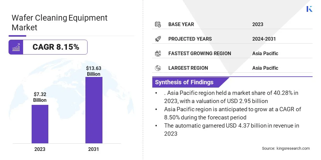
The global wafer cleaning equipment market size was valued at USD 7.32 billion in 2023 and is projected to grow from USD 7.87 billion in 2024 to USD 13.63 billion by 2031, exhibiting a CAGR of 8.15% over the forecast period.
The rapid development of semiconductor production facilities is driving this growth. This growth in semiconductor manufacturing directly contributes to the demand for advanced wafer cleaning equipment, as new facilities require cutting-edge cleaning technologies to maintain yield and ensure optimal product quality during fabrication.
Major companies operating in the wafer cleaning equipment industry are ITW, SEMES, SHIBAURA MECHATRONICS CORPORATION, Beijing TSD Semiconductor Co., Ltd., SCREEN Semiconductor Solutions Co., Ltd., AP&S International GmbH, Veeco Instruments Inc., AXUS TECHNOLOGY, Tokyo Electron Limited, ULTRON SYSTEMS, INC., Modutek Corporation, LAM RESEARCH CORPORATION, Entegris, Akrion Technologies Inc., Applied Materials, Inc.
Moreover, one noticeable trend in the market is the growing preference for single-wafer cleaning systems. As semiconductor devices continue to shrink in size, precise and controlled cleaning processes are becoming essential. Single-wafer cleaning systems provide greater control, ensuring that each wafer meets the highest standards without any damage.
These systems also offer higher efficiency by reducing chemical consumption, making them an ideal for modern, high-precision semiconductor manufacturing environments.
- In June 2024, Fraunhofer IZM-ASSID and EV Group extended their collaboration to further develop wafer bonding technologies for quantum computing applications. Fraunhofer IZM-ASSID installed the EVG850 DB, a fully automated UV laser debonding and cleaning system, at the newly established Center for Advanced CMOS and Heterointegration Saxony in Germany.
Key Highlights:
- The wafer cleaning equipment market size was recorded at USD 7.32 billion in 2023.
- The market is projected to grow at a CAGR of 8.15% from 2024 to 2031.
- Asia Pacific held a market share of 40.28% in 2023, with a valuation of USD 2.95 billion.
- The 300 mm segment garnered USD 3.65 billion in revenue in 2023.
- The wet chemical cleaning process segment is expected to reach USD 5.39 billion by 2031.
- The single wafer spray system segment is expected to reach USD 4.30 billion by 2031.
- The automatic segment is expected to reach USD 8.36 billion by 2031.
- The microelectromechanical systems (MEMS) segment garnered USD 2.16 billion in revenue in 2023.
- North America is anticipated to grow at a CAGR of 8.30% during the forecast period.
Market Driver
Rising Investments in Semiconductor Manufacturing Facilities
The market is being strongly driven by rising investments in semiconductor manufacturing facilities across key global regions. With increasing demand for chips in consumer electronics, automotive, and AI applications, governments and leading semiconductor firms are allocating substantial capital to build new fabs and expand existing ones.
Asia Pacific and North America are particularly seeing large-scale infrastructure developments to boost local chip production and reduce reliance on imports. These expansions will likely fuel the demand for wafer cleaning equipment for ensuring contamination-free wafer surfaces in various stages of semiconductor fabrication.
- In February 2024, the Government of India granted approval for the development of three semiconductor units under the ‘Development of Semiconductors and Display Manufacturing Ecosystems in India’ initiative. These units comprise a semiconductor fabrication plant in Gujarat, an ATMP unit in Assam, and a specialized semiconductor ATMP unit in Gujarat.
Market Challenge
Complexity of Cleaning Advanced Semiconductor Nodes
A major challenge in the wafer cleaning equipment market is the increasing complexity of cleaning advanced semiconductor nodes, especially 5nm and below. As semiconductor devices become smaller and more intricate, traditional cleaning methods may struggle to remove contaminants effectively without damaging delicate surfaces or introducing new defects.
One potential solution to this challenge is the development of advanced cleaning technologies, such as dry cleaning and cryogenic aerosol systems, which offer more precise control and reduce the risk of surface damage. These technologies can achieve effective contaminant removal while being gentle on wafers, ultimately improving cleaning efficiency and yield while reducing the reliance on hazardous chemicals.
Market Trend
Shift Toward Single-Wafer Cleaning Systems
The key market trend in the market is the growing shift toward single-wafer cleaning systems. This trend is largely driven by the increasing need for precise and efficient cleaning processes, especially as semiconductor devices continue to shrink in size.
Single-wafer cleaning systems allow for greater process control, ensuring that each individual wafer is cleaned to the highest standards. This is important for advanced semiconductor nodes, where even the smallest contaminants can lead to performance degradation or yield loss.
The flexibility of single-wafer systems also allows them to be integrated seamlessly into modern semiconductor manufacturing lines, which often require high throughput and adaptability to different wafer sizes and process requirements.
- In November 2024, SCREEN Semiconductor Solutions Co., Ltd. (SCREEN SPE) announced the SS-3200 for 200mm wafers, a new addition to its single wafer cleaning systems utilizing the spin scrubber method. Known for their high cleaning efficiency, stability, and reliability, these systems have helped SCREEN SPE maintain a leading global share in the spin scrubber market.
Wafer Cleaning Equipment Market Report Snapshot
|
Segmentation
|
Details
|
|
By Wafer Size
|
300 mm, 200 mm, ≤ 150 mm
|
|
By Technology
|
Wet Chemical Cleaning Process, Vapor Dry Cleaning Process, Emerging Technologies, Aqueous Cleaning Process, Cryogenic Aerosols & Super-Critical Fluid Cleaning Process
|
|
By Equipment
|
Single Wafer Spray System, Batch Immersion Cleaning Systems, Batch Spray Cleaning System, Ultrasonic Cleaning Equipment, Scrubber, Single Wafer Cryogenic Systems
|
|
By Operation Mode
|
Automatic, Semi-Automatic, Manual
|
|
By Application
|
Microelectromechanical Systems (MEMS), CMOS Image Sensor (CIS), Memory, Logic, Radio Frequency (RF) Devices, Interposer, Light-Emitting Diode (LED), Others
|
|
By Region
|
North America: U.S., Canada, Mexico
|
|
Europe: France, UK, Spain, Germany, Italy, Russia, Rest of Europe
|
|
Asia-Pacific: China, Japan, India, Australia, ASEAN, South Korea, Rest of Asia-Pacific
|
|
Middle East & Africa: Turkey, UAE, Saudi Arabia, South Africa, Rest of Middle East & Africa
|
|
South America: Brazil, Argentina, Rest of South America
|
Market Segmentation:
- By Wafer Size (300 mm, 200 mm, ≤ 150 mm): The 300 mm segment earned USD 3.65 billion in 2023 due to its widespread adoption in advanced semiconductor manufacturing driven by high-volume production needs and improved cost-efficiency per chip.
- By Technology (Wet Chemical Cleaning Process, Vapor Dry Cleaning Process, Emerging Technologies, and Aqueous Cleaning Process): The wet chemical cleaning process held 39.23% of the market in 2023, due to its effectiveness in removing particle and chemical contaminants from wafer surfaces in high-precision processes.
- By Equipment (Single Wafer Spray System, Batch Immersion Cleaning Systems, Batch Spray Cleaning System, and Ultrasonic Cleaning Equipment, Scrubber, Single Wafer Cryogenic Systems ): The Single Wafer Spray System segment is projected to reach USD 4.30 billion by 2031, owing to growing demand for precise, controllable cleaning solutions that support miniaturization and advanced node production.
- By Operation Mode (Automatic, Semi-Automatic, Manual): The automatic segment is projected to reach USD 8.36 billion by 2031, owing to increasing focus on process automation to enhance throughput, consistency, and reduce operational errors.
- By application (Microelectromechanical Systems (MEMS), CMOS Image Sensor (CIS), Memory, Logic, Radio Frequency (RF) Devices, Interposer, Light-Emitting Diode (LED), Others): The microelectromechanical systems (MEMS) segment earned USD 2.16 billion in 2023 due to rising integration of MEMS in consumer electronics, automotive, and industrial applications requiring high wafer cleanliness.
Wafer Cleaning Equipment Market Regional Analysis
Based on region, the global market has been classified into North America, Europe, Asia Pacific, Middle East & Africa, and Latin America.
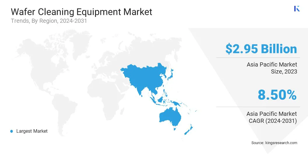
Asia Pacific wafer cleaning equipment market share stood at 40.28% in 2023 in the global market, with a valuation of USD 2.95 billion. This dominance is primarily driven by the presence of major semiconductor manufacturing hubs in China, Taiwan, South Korea, and Japan.
These nations host leading foundries and IDMs that invest in advanced fabrication facilities, driving demand for high-precision wafer cleaning systems. Additionally, strong government initiatives to strengthen domestic semiconductor capabilities, growing electronics exports, and rising consumption of consumer electronics contribute to the region’s market share.
North America is poised to grow at a CAGR of 8.30% over the forecast period. This growth is supported by increased investment in semiconductor manufacturing infrastructure, particularly in theU.S., where strategic initiatives like the CHIPS Act aim to revitalize domestic production.
Government funding, public-private partnerships, and collaborative efforts to reduce reliance on overseas supply chains are further accelerating the expansion of the semiconductor value chain in North America.
- In March 2025, TSMC expanded its investment in advanced semiconductor manufacturing in the U.S by an additional USD 100 billion. This builds upon its existing USD 65 billion investment in Phoenix, Arizona, bringing the company’s total U.S. investment to USD 165 billion. It plans for two advanced packaging facilities, three new fabrication plants, and a major R&D center, marking the largest direct foreign direct investment in U.S. history.
Regulatory Frameworks
- In the U.S, wafer cleaning equipment used in semiconductor manufacturing must comply with standards set by the Occupational Safety and Health Administration (OSHA) and Environmental Protection Agency (EPA), particularly regarding the safe handling and disposal of hazardous chemicals used in wet cleaning processes.
- In Europe, manufacturers must ensure compliance with the EU Machinery Directive (2006/42/EC) and REACH (Registration, Evaluation, Authorisation and Restriction of Chemicals) for chemical usage. Wafer cleaning equipment must also meet CE marking requirements, for conformity with health, safety, and environmental protection standards applicable in the European Economic Area (EEA).
Competitive Landscape:
Companies are heavily focused on developing next-generation cleaning solutions for shrinking device geometries and complex wafer structures, such as 3D NAND and advanced logic nodes. Continuous R&D investment is improving cleaning precision, reducing chemical usage, and enhancing throughput to meet the evolving needs of semiconductor fabs.
Strategic partnerships and collaborations with foundries and integrated device manufacturers (IDMs) are common, enabling equipment providers to co-develop customized cleaning solutions aligned with specific process nodes. In addition, mergers and acquisitions are being used as a key strategy to broaden product portfolios and gain access to complementary technologies, such as cryogenic cleaning systems or environmentally friendly alternatives.
Many companies are also coming up with modular system designs and software-enabled process control to enhance equipment flexibility, reliability, and integration with smart manufacturing environments.
- In November 2024, NexGen Wafer Systems launched SERENO, a high-throughput, multi-chamber platform for clean and wet etch applications. Supporting 6”, 8”, and 12” substrates, SERENO features integrated metrology for precise control of substrate and layer thickness, as well as surface roughness. With a compact footprint of under 12 m² and a throughput of up to 200 wafers per hour, it offers flexible chemical handling and analytics for FEOL and BEOL applications.
List of Key Companies in Wafer Cleaning Equipment Market:
- ITW
- SEMES
- SHIBAURA MECHATRONICS CORPORATION
- Beijing TSD Semiconductor Co., Ltd.
- SCREEN Semiconductor Solutions Co., Ltd.
- AP&S International GmbH
- Veeco Instruments Inc.
- AXUS TECHNOLOGY
- Tokyo Electron Limited
- ULTRON SYSTEMS, INC.
- Modutek Corporation
- LAM RESEARCH CORPORATION
- Entegris
- Akrion Technologies Inc.
- Applied Materials, Inc.
Recent Developments (Product Launch)
- In December 2024, Tokyo Electron launched Ulucus LX, a Laser Lift Off system designed for 300mm wafer-bonded devices. The system addresses the growing demand for 3D integration and permanent wafer bonding in advanced semiconductor devices, particularly in the AI era. Ulucus LX combines wafer removal, laser beam irradiation, and cleaning within a single unit, enhancing both sustainability and productivity. It integrates advanced laser control, wafer separation, and cleaning technologies from TEL’s NS and CELLESTA series, as well as the LITHIUS Pro Z Coater/Developer platform.


