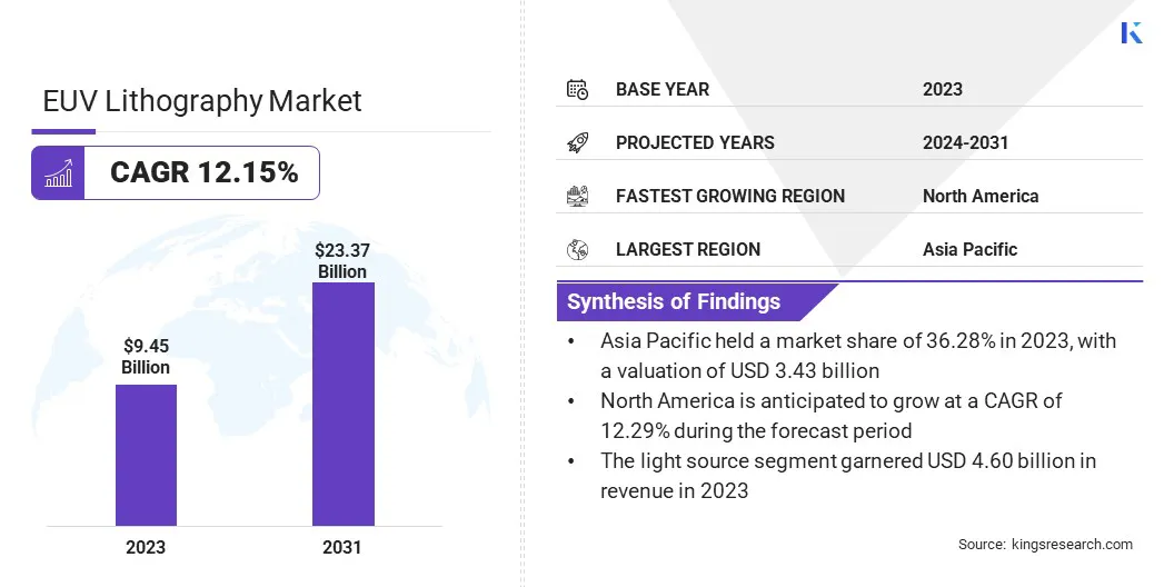
EUV Lithography Market Size
The global EUV Lithography Market size was valued at USD 9.45 billion in 2023 and is projected to grow from USD 10.47 billion in 2024 to USD 23.37 billion by 2031, exhibiting a CAGR of 12.15% during the forecast period. The rapid adoption of technologies like artificial intelligence (AI), the Internet of Things (IoT), and 5G technology is fueling the need for cutting-edge semiconductor devices.
EUV lithography is essential in this context, as it enables the production of smaller, more powerful, and energy-efficient chips. These advanced chips are crucial for powering next-generation technologies, including AI-driven applications and high-speed 5G networks.
In the scope of work, the report includes products and services offered by companies such as ASML, Nikon Corporation, Ushio Inc., Photronics Inc., TRUMPF, Taiwan Semiconductor Manufacturing Company Limited, Toppan Photomasks Inc., Carl Zeiss AG, KLA Corporation, SUSS MicroTec SE, and others.
Moreover, the increasing need for high-performance computing, driven by data centers, cloud computing, and AI applications, is propelling the growth of the EUV lithography market. The technology enables the production of high-density chips required to meet the stringent performance and energy efficiency demands of these applications. As both businesses and consumers seek faster and more efficient computing solutions, the demand for EUV lithography is poised to rise.
EUV (Extreme Ultraviolet) lithography is an advanced semiconductor manufacturing process that uses extreme ultraviolet light with a wavelength of 13.5 nanometers to etch intricate and highly dense circuit patterns onto silicon wafers. This technology is crucial for producing smaller, faster, and more power-efficient microchips, which are essential for modern electronics such as smartphones, high-performance computing, and 5G networks.
EUV lithography allows for greater precision and miniaturization compared to traditional lithography methods, enabling the development of next-generation semiconductors that drive technological advancements across various industries.
Analyst’s Review
The robust network of collaborations among leading technology companies, lithography providers, research institutions, and government agencies is essential for advancing EUV lithography technology. These strategic partnerships are contributing significantly to market growth. Collaborations between the companies are crucial for advancing the boundaries of EUV lithography, a technology critical for the production of smaller, more powerful, and energy-efficient semiconductor devices.
These partnerships are enabling the development of cutting-edge lithography techniques that are essential for the next generation of semiconductor manufacturing. The collaborative efforts are enhancing the capabilities of EUV technology and increasing its integration into various applications, thereby supporting the expansion of the market.
Furthermore, semiconductor foundries are rapidly incorporating EUV lithography into their operations due to its critical role in producing advanced semiconductor devices. EUV technology enables the fabrication of smaller and more complex semiconductor features, which are essential for meeting the increasing demand for higher performance and lower power consumption in electronics. As foundries adopt EUV lithography, they enhance their ability to manufacture cutting-edge chips with improved precision and efficiency.
- For instance, in April 2024, Intel Foundry installed the industry's first commercial High Numerical Aperture (High NA) Extreme Ultraviolet (EUV) lithography scanner at its R&D facility in Hillsboro, Oregon. The TWINSCAN EXE:5000 High NA EUV tool, provided by lithography leader ASML is anticipated to facilitate unparalleled scalability and precision in chip manufacturing for Intel. This advanced technology allows Intel to manufacture chips with cutting-edge capabilities and features, which are crucial foradvancing innovation in emerging technologies, including AI.
EUV Lithography Market Growth Factors
The global demand for microchips is increasing due to the widespread adoption of advanced technologies such as artificial intelligence, 5G, and the Internet of Things (IoT). As industries increasingly rely on more powerful and efficient electronic devices, there is a corresponding need for smaller, more sophisticated microchips.
Semiconductor miniaturization has become a critical focus, enabling the production of compact and highly efficient devices that deliver enhanced performance. EUV lithography plays an indispensable role in this miniaturization process, allowing manufacturers to create ultra-fine circuit patterns with unprecedented precision.
This capability is essential for producing the next generation of microchips that meet the stringent requirements of modern applications. The growing emphasis on miniaturization is augmenting the expansion of the EUV lithography market, as it supports the development of cutting-edge semiconductors that are foundational to technological innovation.
Moreover, governments worldwide are placing growing emphasis on the semiconductor industry, recognizing its significance in national security and economic competitiveness. To advance domestic chip manufacturing, they are offering substantial support through funding, tax incentives, and strategic initiatives.
This governmental support is particularly strong in countries such as the U.S., Europe, and China, where efforts are focused on strengthening the semiconductor supply chain and advancing local production capabilities. There is a major shift toward adopting cutting-edge technologies such as EUV lithography, which is essential for producing next-generation semiconductors.
- For instance, in May 2024, the Chinese governmentintroduced its state-backed third planned investment fund to expand its semiconductor industry,. This fund, with a capital of USD 47.5 billion,was detailed in a filing with a government-operated company registry.
EUV Lithography Market Trends
The ongoing advancement of EUV lithography technology is a significant trend propelling market growth, particularly through its enhanced capabilities in semiconductor manufacturing. Key innovations in EUV source technology have led to increased source power and productivity, thereby enabling higher wafer yields.
These improvements are crucial for meeting the rising demand for advanced chips. Progress in producing defect-free and more durable masks is resulting in the widespread adoption of this technology. Moreover, the development of next-generation EUV lithography scanners, which offer higher resolution and improved overlay accuracy, is advancing the limits of miniaturization and boosting performance in chip production.
These technological advancements are improving efficiency and cost-effectiveness while also setting new standards for precision and capability in semiconductor fabrication, thereby augmenting the expansion of the EUV lithography market.
Additionally, the continuous advancement within the consumer electronics industry is a major trend fueling the growth of market. As consumers increasingly demand devices with superior performance, extended battery life, and innovative features, there has been a significant rise in the need for advanced semiconductor chips.
EUV lithography plays a pivotal role in this transformation, enabling the production of ultra-compact, high-performance chips that are critical for next-generation smartphones, laptops, gaming consoles, and wearables. This technology enables manufacturers to redefine the possibilities in consumer electronics, delivering state-of-the-art products that meet the increasing expectations of tech-savvy consumers.
As competition to offer the most advanced devices intensifies, the role of EUV lithography in consumer electronics becomes increasingly critical.
- According to the Gitnux Org. Report, the global consumer electronics market was valued at USD 729.11 billion in 2022 and is projected to grow at a CAGR of 6.9% from 2023 to 2030.
Segmentation Analysis
The global market is segmented based on equipment, end-user, and geography.
By Equipment
Based on equipment, the market is segmented into light source, optics, and others. The light source segment led the EUV lithography market in 2023, reaching a valuation of USD 4.60 billion. This prominence is attributed to its critical role in enabling the entire lithography process. The light source generates the extreme ultraviolet (EUV) light required for etching precise patterns onto silicon wafers.
As semiconductor manufacturers continue to advance miniaturization, the demand for more powerful and efficient light sources has significantly increased. This dominance is further reinforced by the significant R&D investments and high production costs associated with developing and maintaining these advanced light sources.
By End-User
Based on end-user, the market is classified into integrated device manufacturers and foundries. The foundries segment secured the largest revenue share of 58.72% in 2023 due to its significant role in the mass production of semiconductor chips. Foundries are the primary adopters of EUV lithography technology.
The demand for smaller, more efficient chips used in advanced applications such as AI, 5G, and high-performance computing has prompted foundries to invest heavily in EUV lithography. This technology enables them to produce the intricate and high-density patterns required for these next-generation semiconductors.
Additionally, foundries are consistently required to deliver higher performance and foster innovation on a large scale, rendering EUV lithography indispensable in meeting the growing market demands.
EUV Lithography Market Regional Analysis
Based on region, the global market is classified into North America, Europe, Asia-Pacific, MEA, and Latin America.
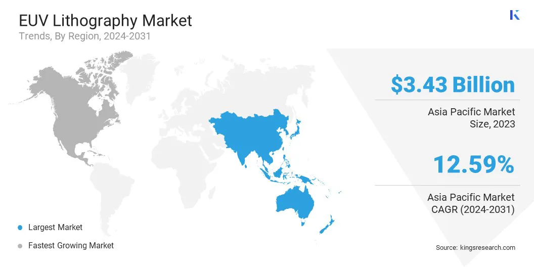
Asia Pacific EUV lithography market accounted for a substantial share of around 36.28% in 2023, with a valuation of USD 3.43 billion. Asia-Pacific, particularly countries such as Taiwan, South Korea, and China, is home to some of the world's largest and most advanced semiconductor manufacturers.
These companies are increasingly adopting EUV lithography to maintain their competitive edge and address the rising global demand for cutting-edge chips. The region's dominance in semiconductor production fuels the need for advanced lithography equipment, thereby supporting regional market growth.
- According to the Asian Development Bank, high-income and developing economies in East Asia and Southeast Asia collectively represent over 80% of global semiconductor manufacturing. Japan hosts some of the largest companies that supply equipment and materials essential for thesemiconductor industry, whereas the People’s Republic of China leads the world in the production of photovoltaic cells, another important category of semiconductors.
The Asia-Pacific region is a major hub for consumer electronics manufacturing, with companies in this region responsible for producing a significant share of the world's smartphones, laptops, and other electronic devices. The growing demand for these products, coupled with the shift toward more advanced and efficient semiconductors, is leading to the widespread adoption of EUV lithography to produce the next generation of chips.
- A report co-released by global accounting firm Ernst & Young and the China Chamber of Commerce for Import and Export of Machinery and Electronic Products in 2024 highlights China's emergence as a global hub for consumer electronics and household appliances. In 2023, China dominated the Asia-Pacific market, capturing approximately 48% of sales share. The report underscores that China hassolidified its position as a leading nation in both production and sales and maintained a significant presence in exports, accounting for 42% of global export shares in 2022.
North America is poised to witness significant growth at a robust CAGR of 12.29% over the forecast period. The U.S. government has been increasingly focused on boosting domestic semiconductor manufacturing to enhance national security and reduce reliance on foreign suppliers.
Initiatives such as the CHIPS Act, which provides substantial funding and incentives for semiconductor manufacturing and research, are boosting the adoption of advanced technologies such as EUV lithography in North America.
- According to an August 2024 report by the East Asia Forum, the semiconductor industry has emerged as a crucial component of the U.S. economy and national security. This is evidenced by the rapid expansion of semiconductor manufacturing facilities nationwide. Significant investments, such as Intel's new Fab 42 facility and TSMC's factory in Arizona, are bolstering domestic production capabilities. Although the United States holds only 12 percent of global manufacturing capacity, it accounts for over 46 percent of total semiconductor sales in 2024, highlighting its significant influence in the global market. The Semiconductor Industry Association has reported that the CHIPS Act hasstimulated over USD 450 billion in private investments in the U.S. semiconductor sector, leading to 83 new semiconductor ecosystem projects across 25 states.
Moreover, the region’s semiconductor industry benefits from a strong network of collaborations between leading technology companies, research institutions, and government agencies. These partnerships are advancing EUV lithography and facilitating its adoption across various applications, thereby boosting the expansion of the North America market.
Competitive Landscape
The global EUV Lithography market report will provide valuable insight with an emphasis on the fragmented nature of the industry. Prominent players are focusing on several key business strategies such as partnerships, mergers and acquisitions, product innovations, and joint ventures to expand their product portfolio and increase their market shares across different regions.
Strategic initiatives, including investments in R&D activities, the establishment of new manufacturing facilities, and supply chain optimization, could create new opportunities for market growth.
List of Key Companies in EUV Lithography Market
Key Industry Developments
- June 2024 (Partnership): ASML, in partnership with Imec, an innovation and research hub digital technologies, announced the inauguration of the High NA EUV Lithography Lab in Netherlands. This advanced facility, operated jointly by the two companies, isdesigned toprovide cutting-edge memory chip manufacturers with access to the first prototype High NA EUV scanner, along with the associated metrology and processing tools.
- February 2024 (Joint Venture): Toppan Photomask, a leading global provider of semiconductor photomasks, announced a joint research and development agreement with IBM. This collaboration is focused on advancing the 2 nanometer (nm) logic semiconductor node through the use of extreme ultraviolet (EUV) lithography. Additionally, the partnership includes efforts to develop High-NA EUV photomasks for next-generation semiconductors.
The global EUV Lithography market is segmented as:
By Equipment
- Light Source
- Optics
- Others
By End-User
- Integrated Device Manufacturers
- Foundries
By Region
- North America
- Europe
- France
- U.K.
- Spain
- Germany
- Italy
- Russia
- Rest of Europe
- Asia-Pacific
- China
- Japan
- India
- South Korea
- Rest of Asia-Pacific
- Middle East & Africa
- GCC
- North Africa
- South Africa
- Rest of Middle East & Africa
- Latin America
- Brazil
- Argentina
- Rest of Latin America


