Market Definition
The market encompasses software tools and services used for designing, simulating, and testing electronic systems such as integrated circuits (ICs) and printed circuit boards (PCBs).
It includes a wide range of solutions for schematic capture, layout design, verification, and simulation, for consumer electronics, automotive, telecommunications, and aerospace industries. The report analyzes key market drivers, regional dynamics, and the competitive landscape expected to shape the market during the forecast period.
Electronic Design Automation Market Overview
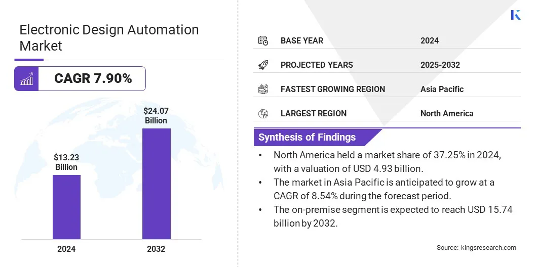
The global electronic design automation market size was valued at USD 13.23 billion in 2024 and is projected to grow from USD 14.14 billion in 2025 to USD 24.07 billion by 2032, exhibiting a CAGR of 7.90% during the forecast period.
The market is expanding rapidly, fueled by increasing investments in advanced manufacturing technologies and the shift toward automation in electronics design. The continuous need for higher design accuracy, faster time-to-market, and improved performance in electronic products is fueling demand for sophisticated EDA tools.
Major companies operating in the electronic design automation indusry are Synopsys, Inc., Cadence Design Systems, Inc., Siemens, ANSYS, Inc, Keysight Technologies, Renesas Electronics Corporation, Zuken, AGNISYS, INC., Aldec, Inc., Codasip, Secure-IC, Autodesk Inc., EasyEDA, Eremex Inc, and Pulsic Limited.
Additionally, the expansion of semiconductor manufacturing and the shift toward customized, application-specific integrated circuits (ASICs) are driving market growth. Cloud-based EDA solutions are gaining adoption across sectors such as consumer electronics, automotive, and telecommunications due to their flexibility, scalability, and support for complex design workflows, thereby driving market growth.
- In March 2024, HCLTech launched an Electronic Design Automation (EDA) solution in partnership with NetApp to accelerate EDA implementations in the hybrid cloud. The solution uses NetApp’s Design Anywhere platform to streamline semiconductor design, improve scalability, and manage infrastructure orchestration for large EDA workloads.
Key Highlights
- The electronic design automation market size was valued at USD 13.23 billion in 2024.
- The market is projected to grow at a CAGR of 7.90% from 2025 to 2032.
- North America held a market share of 37.25% in 2024, with a valuation of USD 4.93 billion.
- The semiconductor IP segment garnered USD 5.03 billion in revenue in 2024.
- The on-premise segment is expected to reach USD 15.74 billion by 2032.
- The automotive segment is expected to reach USD 5.94 billion by 2032.
- The market in Asia Pacific is anticipated to grow at a CAGR of 8.54% during the forecast period.
Market Driver
Increasing Complexity of Semiconductor Designs Driving Demand for Advanced EDA Tools
The market is experiencing significant growth driven by the increasing complexity of semiconductor designs. As the industry shifts toward advanced node technologies and multi-die systems, there is a growing demand for more sophisticated EDA tools that can streamline the design, verification, and simulation processes.
EDA tools play a pivotal role in optimizing the design flow, ensuring functional correctness, and enabling performance optimization across diverse applications. The evolving need for tools that support new materials, shrinking nodes, and the integration of multiple chips in a single system is driving demand for next-generation EDA solutions, in turn driving the growth of the market.
- In September 2024, Synopsys, Inc. and TSMC collaborated to deliver advanced EDA and IP solutions on TSMC's cutting-edge processes and 3DFabric technologies. The partnership aimed to accelerate innovation in AI and multi-die chip design by leveraging AI-driven EDA flows, new backside power delivery capabilities, and multi-physics solutions to enhance performance, power efficiency, and engineering productivity.
Market Challenge
Cybersecurity Challenges
Cybersecurity is a major challenge in the electronic design automation market, as the increasing complexity of semiconductor designs makes them more vulnerable to cyberattacks.
EDA tools are integral in designing and verifying chips, and these tools often handle sensitive intellectual property and proprietary designs. As designs move across cloud environments and collaborative platforms, the risk of cyber threats such as data breaches, IP theft, and sabotage has grown.
To address these threats, EDA providers are adopting advanced cybersecurity solutions. This includes implementing robust encryption methods to protect design data, using secure cloud platforms with built-in protection, and introducing strong user authentication protocols.
- In January 2025, Secure-IC joined Cadence Design Systems, Inc., a global leader in electronic design automation, to become its dedicated security entity. The acquisition integrates Secure-IC’s embedded cybersecurity solutions into Cadence’s EDA portfolio. This enhances Cadence’s capabilities in secure chiplet and complex SoC design, helping address the growing need for hardware-level security in the semiconductor design process.
Market Trend
AI and Machine Learning Enhancing Efficiency and Optimization
The integration of AI and machine learning into electronic design automation workflows is a prominent trend reshaping the market. This technological shift enables faster design cycles by automating complex processes and optimizing design efficiency.
Additionally, AI and machine learning enhance performance-power-area optimization, allowing for improved chip performance while minimizing power consumption and area requirements. The automation of verification processes further reduces manual intervention, improving accuracy and reducing the time-to-market for new designs.
As a result, these advancements are significantly boosting productivity, empowering engineers to meet the increasing demand for more complex and efficient semiconductor designs in the market.
- In March 2024, Synopsys, Inc. introduced new AI-driven EDA, IP, and systems design solutions at the SNUG Silicon Valley conference, California. These included 3DSO.ai for 3D design space optimization, new hardware-assisted verification systems, and a hybrid cloud solution for EDA workflows.
Electronic Design Automation Market Report Snapshot
|
Segmentation
|
Details
|
|
By Tool Type
|
Semiconductor IP, Computer-Aided Engineering (CAE), IC Physical Design & Verification, Printed Circuit Board (PCB) & MCM, Design for Manufacturing (DFM), Others
|
|
By Deployment
|
On-premise, Cloud-based
|
|
By End-use Industry
|
Consumer Electronics, Automotive, Industrial, Telecom & Networking, Aerospace & Defense, Others
|
|
By Region
|
North America: U.S., Canada, Mexico
|
|
Europe: France, UK, Spain, Germany, Italy, Russia, Rest of Europe
|
|
Asia-Pacific: China, Japan, India, Australia, ASEAN, South Korea, Rest of Asia-Pacific
|
|
Middle East & Africa: Turkey, U.A.E., Saudi Arabia, South Africa, Rest of Middle East & Africa
|
|
South America: Brazil, Argentina, Rest of South America
|
Market Segmentation
- By Tool Type (Semiconductor IP, Computer-Aided Engineering (CAE), IC Physical Design & Verification, Printed Circuit Board (PCB) & MCM, Design for Manufacturing (DFM), and Others): The semiconductor IP segment earned USD 5.03 billion in 2024 due to the increasing demand for high-performance, customized chips for advanced technologies like 5G and IoT.
- By Deployment (On-premise, Cloud-based): The on-premise segment held 65.91% of the market in 2024, due to the preference for greater control, data security, and integration with legacy systems in highly regulated industries.
- By End-use Industry (Consumer Electronics, Automotive, Industrial, Telecom & Networking, Aerospace & Defense, Others): The automotive segment is projected to reach USD 5.94 billion by 2032, owing to the increasing demand for advanced driver-assistance systems (ADAS) and electric vehicle (EV) technologies that require complex circuit designs.
Electronic Design Automation Market Regional Analysis
Based on region, the market has been classified into North America, Europe, Asia Pacific, Middle East & Africa, and South America.
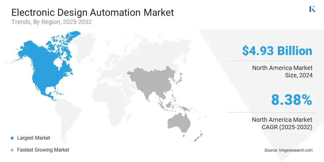
North America accounted for 37.25% share of the electronic design automation market in 2024, with a valuation of USD 4.93 billion. The region’s dominance is primarily driven by the presence of major semiconductor and electronics companies, including global leaders in consumer electronics, automotive, and telecommunications.
The demand for advanced EDA tools in industries such as aerospace and defense is also contributing significantly to the market growth in this region.
Furthermore, the adoption of cloud-based EDA solutions is enhancing operational efficiency and time-to-market of semiconductor chips and electronic devices. These factors are accelerating product development cycles, in turn, driving growth in the market.
- In December 2024, Marvell Technology, Inc. collaborated with Amazon Web Services (AWS) through a five-year agreement. The partnership focuses on utilizing AWS cloud infrastructure for Marvell’s electronic design automation (EDA) to accelerate silicon design and enhance data center semiconductor solutions.
The electronic design automation industry in Asia Pacific is expected to register the fastest growth in the market, with a projected CAGR of 8.54% over the forecast period. This growth is driven by the rapidly expanding semiconductor manufacturing sector in countries like China, Taiwan, South Korea, and Japan, which are hubs for global semiconductor production.
The rising demand for consumer electronics, including smartphones, wearables, and IoT devices, is increasing the need for advanced EDA tools for IC design and PCB layout. Additionally, the region's focus on automotive innovation, particularly in electric vehicles (EVs) and autonomous driving technologies, is further boosting the demand for advanced EDA solutions.
Regulatory Frameworks
- In the U.S., the regulatory body for the semiconductor industry is the U.S. Department of Commerce (DOC), through its various bureaus and divisions like the National Institute of Standards and Technology (NIST).
- In Europe, the semiconductor ecosystem is guided by the European Commission, which launched the European Chips Act to bolster chip production and reduce dependency on foreign suppliers. While it does not directly regulate the electronic design market, the Act influences it by funding R&D, facilitating public-private partnerships, and coordinating efforts through the European Semiconductor Board (ESB) to implement strategic goals across member states.
Competitive Landscape
Companies in the global electronic design automation market are actively pursuing mergers, acquisitions, and strategic collaborations to strengthen their market positions and broaden technological capabilities. Many are forming partnerships with cloud service providers to support the development and deployment of cloud-based EDA platforms.
Firms are also expanding their product lines by introducing domain-specific tools tailored for sectors such as automotive, aerospace, and telecommunications. Increased investments in research and development are common, along with joint ventures and alliances with universities and research institutions.
Additionally, several players are entering new geographic markets and establishing regional design centers to diversify their global footprint and access local talent.
- In October 2024, Siemens Digital Industries Software and CELUS collaborated to integrate AI-powered automation into PCB design. The partnership aimed to simplify complex PCB design processes for small and medium-sized businesses by combining Siemens’ EDA tools with CELUS’ AI-driven automation platform.
List of Key Companies in Electronic Design Automation Market:
- Synopsys, Inc.
- Cadence Design Systems, Inc.
- Siemens
- ANSYS, Inc
- Keysight Technologies
- Renesas Electronics Corporation
- Zuken
- AGNISYS, INC.
- Aldec, Inc.
- Codasip
- Secure-IC
- Autodesk Inc.
- EasyEDA
- Eremex Inc
- Pulsic Limited
Recent Developments (Collaboration/Software Launch)
- In March 2025, Synopsys Inc. and NVIDIA entered a multi-year collaboration to accelerate electronic design automation (EDA) workflows using the NVIDIA Grace Blackwell platform, with expected performance improvements of up to 30 times for circuit simulation and 20 times for computational lithography.
- In November 2024, Keysight Technologies, Inc. launched its electronic design automation software portfolio to accelerate radio frequency (RF) circuit design, high-speed digital simulations, and device modeling. The suite integrates artificial intelligence, machine learning, and Python-based workflows to reduce RF modeling time and streamline chiplet interconnect design.


