Market Definition
The market encompasses a diverse range of materials essential used in device fabrication and packaging. This market includes silicon wafers, electronic gases for processes such as deposition, etching, and doping, and photomasks for precise pattern transfer in photolithography.
The report highlights key factors influencing the market , along with an in-depth analysis of emerging trends and the evolving regulatory frameworks shaping the industry's trajectory.
Semiconductor Materials Market Overview
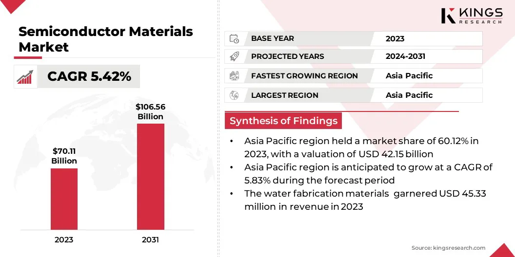
The global semiconductor materials market size was valued at USD 70.11 billion in 2023 and is projected to grow from USD 73.66 billion in 2024 to USD 106.56 billion by 2031, exhibiting a CAGR of 5.42% during the forecast period.
Market growth is fueled by ongoing technological advancements and increasing demand from various high-tech industries. The proliferation of artificial intelligence (AI), 5G connectivity, and high-performance computing (HPC) is driving the need for advanced semiconductor chips, leading to a surge in the consumption of high-purity silicon wafers, photolithography materials, and specialty electronic gases.
Major companies operating in the semiconductor materials industry are Tekscend Photomask, SOITEC, Siltronic, Mitsui Chemicals India Pvt. Ltd., SK Inc., SHINKO ELECTRIC INDUSTRIES CO., LTD., Unimicron, GlobalWafers, Nitto Denko Corporation, Heraeus Electronics, Photronics, Inc., SUMCO CORPORATION, Fujimi Incorporated, Tokyo Ohka Kogyo Co., Ltd., Shin-Etsu Chemical Co., Ltd., and others.
Furthermore, the global transition to advanced packaging technologies, including 3D ICs, chiplets, and heterogeneous integration, is reshaping semiconductor design and manufacturing. These methods are critical for enhancing performance and miniaturization without relying solely on traditional lithographic scaling.
- In March 2025, the Semiconductor Industry Association (SIA) acknowledged TSMC's announcement to increase its U.S. investment in advanced semiconductor manufacturing to USD 165 billion. The expansion includes three new fabs, two advanced packaging facilities, and an R&D center to enhance domestic chip production and support emerging technologies such as AI.
Key Highlights:
- The semiconductor materials industry size was recorded at USD 70.11 billion in 2023.
- The market is projected to grow at a CAGR of 5.42% from 2024 to 2031.
- Asia Pacific held a share of 60.12% in 2023, valued at USD 42.15 billion.
- The silicon wafers segment garnered USD 23.14 billion in revenue in 2023.
- The leadframe segment is expected to reach USD 28.75 billion by 2031.
- The wafer fabrication materials segment is estimated to generate a value of USD 67.06 billion by 2031.
- The consumer electronics segment is likely to reach USD 49.46 billion by 2031.
- Europe is anticipated to grow at a CAGR of 5.41% over the forecast period.
Market Driver
Rising Demand for AI, 5G, and High-Performance Computing
The market is witnessing significant growth, fueled by the rising demand for AI, 5G, and high-performance computing (HPC) applications. The adoption of AI-based data processing, cloud computing, and edge devices is highlighting the need for advanced semiconductor chips, thereby boosting the use of high-purity silicon wafers, electronic gases, and photolithography materials.
Additionally, the global expansion of 5G networks is accelerating the production of radio frequency (RF) semiconductors and power electronics, increasing demand for specialty semiconductor materials. As AI and 5G technologies evolve, the demand for next-generation semiconductor materials is expected to grow, reinforcing their critical role in supporting technological advancements.
- In November 2024, according to the Ericsson Mobility Report, 5G subscriptions continued eise, with projections indicating that one-quarter of all mobile subscriptions will be 5G-enabled by year-end. The report further forecasts 5G will surpass 4G as the dominant mobile access technology by 2027.
Market Challenge
Supply Chain Disruptions and Raw Material Shortages
The expansion of the semiconductor materials market is impeded by supply chain disruptions and raw material shortages, mainly due to geopolitical tensions, trade restrictions, and fluctuating demand. Critical materials such as high-purity silicon wafers, electronic gases, and rare earth metals are highly concentrated in a few regions, making the industry vulnerable to supply constraints and price volatility.
These disruptions can lead to production delays and increased costs, affecting semiconductor manufacturers worldwide. To mitigate these challenges, industry players are prioritizing the localization of semiconductor material production, with substnatial investments in regional supply chains, strategic stockpiling, and alternative material sourcing.
Market Trend
Shift Toward Advanced Packaging Technologies
The market is witnessing a major transition to advanced packaging technologies such as 3D ICs, chiplets, and heterogeneous integration. These innovations are reshaping the industry by enabling higher transistor densities, improved power efficiency, and enhanced computing performance without solely relying on traditional lithographic scaling.
3D ICs require specialized bonding wires, encapsulation resins, and substrates to ensure reliable interconnectivity and thermal dissipation. Meanwhile, chiplet-based architectures are highlighting the increased need for high-density interposers and advanced underfill materials.
This shift is prompting material suppliers to develop low-resistance interconnects, enhanced thermal interface materials, and highly reliable die-attach solutions, which are crucial for supporting the next generation of semiconductors
- In July 2023, Applied Materials, Inc. unveiled advanced materials, technologies, and systems designed to support the integration of chiplets into sophisticated 2.5D and 3D packages through hybrid bonding and through-silicon vias (TSVs). These innovations enhanced Applied’s capabilities in heterogeneous integration (HI), allowing semiconductor manufacturers to seamlessly combine chiplets of different functions, technology nodes, and sizes into a single, cohesive product.
Semiconductor Materials Market Report Snapshot
|
Segmentation
|
Details
|
|
By Material Type
|
Silicon Wafers, Electronic Gases, Photomasks, Photoresists and Adjacent Chemicals, CMP (Chemical Mechanical Planarization) Materials, SOI (Silicon on Insulator) Wafers, Other Specialty Materials
|
|
By Packaging Type
|
Leadframe, Substrates, Bonding Wires, Encapsulation Resins, Die Attach and Thermal Interface Materials
|
|
By Application
|
Wafer Fabrication Materials, Packaging Materials
|
|
By End-Use Industry
|
Consumer Electronics, Automotive, Industrial Automation, Telecommunications, Healthcare, Aerospace & Defense
|
|
By Region
|
North America: U.S., Canada, Mexico
|
|
Europe: France, UK, Spain, Germany, Italy, Russia, Rest of Europe
|
|
Asia-Pacific: China, Japan, India, Australia, ASEAN, South Korea, Rest of Asia-Pacific
|
|
Middle East & Africa: Turkey, UAE, Saudi Arabia, South Africa, Rest of Middle East & Africa
|
|
South America: Brazil, Argentina, Rest of South America
|
Market Segmentation
- By Material Type (Silicon Wafers, Electronic Gases, Photomasks, Photoresists and Adjacent Chemicals, and CMP (Chemical Mechanical Planarization) Materials, SOI (Silicon on Insulator) Wafers, and Other Specialty Materials): The silicon wafers segment earned USD 23.14 billion in 2023 due to the increasing demand for advanced semiconductor nodes in consumer electronics and automotive applications.
- By Packaging Type (Leadframe, Substrates, Bonding Wires, and Encapsulation Resins): The leadframe segment held a share of 29.15% in 2023, largely attributed to its widespread use in high-power and cost-effective semiconductor packaging solutions.
- By Application (Wafer Fabrication Materials and Packaging Materials): The wafer fabrication materials segment is projected to reach USD 67.06 billion by 2031, on account of the rising adoption of advanced lithography and scaling technologies in semiconductor manufacturing.
- By End-Use Industry (Consumer Electronics, Automotive, Industrial Automation, and Telecommunications): The consumer electronics segment is estimated to generate a revenue of USD 49.46 billion by 2031, fueled by the growing demand for high-performance computing, smartphones, and smart devices.
Semiconductor Materials Market Regional Analysis
Based on region, the global market has been classified into North America, Europe, Asia Pacific, Middle East & Africa, and Latin America.
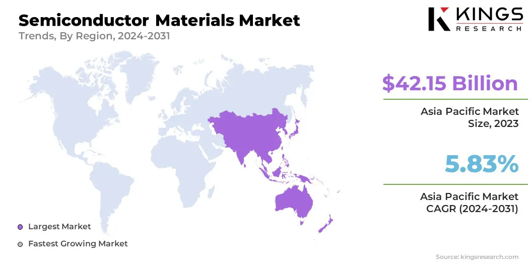
Asia Pacific semiconductor materials market share stood at around 60.12% in 2023, valued at USD 42.15 billion. This dominance is supported by the presence of leading semiconductor manufacturing hubs, particularly in China, Taiwan, South Korea, and Japan.
The rapid expansion of foundries and integrated device manufacturers (IDMs), coupled with government incentives supporting domestic semiconductor production, is further fueling this growth. Additionally, the growing demand for consumer electronics, electric vehicles (EVs), and industrial automation is underscoring the need for advanced semiconductor materials.
The presence of major semiconductor fabrication facilities, along with a well-established supply chain for materials such as silicon wafers, photomasks, and electronic gases, is reinforcing the region's leading position.
- In April 2025, the Government of India approved the Semicon India programme to strengthen the country's semiconductor and display manufacturing ecosystem. The initiative offers fiscal support covering 50% of the project cost for establishing Silicon CMOS-based semiconductor and display fabrication units. Additionally, it provides 50% capital expenditure assistance for compound semiconductors, silicon photonics, sensors, discrete semiconductor fabs, and semiconductor ATMP/OSAT facilities.
Europe semiconductor materials industry is poised to grow at a CAGR of 5.41% over the forecast period. This rapid growth is bolstered by the region's strong research and development (R&D) infrastructure, advanced chip design capabilities, and growing semiconductor manufacturing capacity.
Government policies aimed at strengthening domestic semiconductor production and reducing supply chain dependencies are significantly contributing to this growth. The rising demand for AI, 5G technology, automotive electronics, and high-performance computing (HPC) is fueling the need for high-quality semiconductor materials. Additionally, the regional market benefits from strong expertise in electronic gases, CMP materials, photolithography, and advanced packaging solutions
Regulatory Frameworks
- In the U.S., the Environmental Protection Agency (EPA) and the Occupational Safety and Health Administration (OSHA) regulate the semiconductor materials industry by overseeing the handling, use, and disposal of hazardous chemicals involved in semiconductor manufacturing.
- In Europe, the Registration, Evaluation, Authorisation, and Restriction of Chemicals (REACH) Regulation governs the use of chemicals in semiconductor materials to ensure environmental and human health safety. The Restriction of Hazardous Substances (RoHS) Directive limits the use of hazardous substances in electronic components, including semiconductor materials, while the European Chips Act aims to strengthen semiconductor supply chains within the region.
Competitive Landscape
Companies operating in the semiconductor materials market are investing heavily in R&D to enhance the performance, purity, and efficiency of materials such as silicon wafers, photoresists, and CMP slurries, catering to the demands of advanced semiconductor nodes.
Key efforts include strategic collaborations with semiconductor foundries and integrated device manufacturers (IDMs), enabling material suppliers to align their innovations with next-generation chip fabrication requirements. Additionally, several companies are expanding manufacturing facilities in key regions to ensure a stable supply chain and mitigate geopolitical risks.
Furthermore, mergers and acquisitions are shaping the competitive landscape, with firms acquiring specialized material manufacturers to broaden their product portfolios and enhance technical expertise. Developing eco-friendly and regulatory-compliant materials is allowing companies to meet environmental standards and reduce the carbon footprint of semiconductor manufacturing.
Furthermore, localized production strategies, supported by government incentives, are being employed to reduce dependence on foreign suppliers and ensure resilience in semiconductor material sourcing.
- In October 2024, Infineon Technologies AG announced the development of the world’s thinnest silicon power wafer at 20 micrometers in thickness. This breakthrough enables a 15 percent reduction in power losses by cutting substrate resistance in half.
List of Key Companies in Semiconductor Materials Market:
- Tekscend Photomask
- SOITEC
- Siltronic
- Mitsui Chemicals India Pvt. Ltd.
- SK Inc.
- SHINKO ELECTRIC INDUSTRIES CO., LTD.
- Unimicron
- GlobalWafers
- Nitto Denko Corporation
- Heraeus Electronics
- Photronics, Inc.
- SUMCO CORPORATION
- Fujimi Incorporated
- Tokyo Ohka Kogyo Co., Ltd.
- Shin-Etsu Chemical Co., Ltd.
Recent Developments (Program Commencement)
- In September 2024, Applied Materials India introduced the Applied Semiconductor Collaboration in Engineering and Technology (ASCENT) initiative. This annual program is designed to advance innovation and education in semiconductor equipment by fostering collaboration between researchers from select universities and Applied India engineers. It aims to accelerate the development of cutting-edge technologies to address the industry's most complex technical challenges.


