Market Definition
The market encompasses the global ecosystem of manufacturers, suppliers, service providers, and end users engaged in the development, distribution, and application of SEM technology.
This market is driven by the rising demand for high-resolution imaging and material characterization across key industries, including semiconductors, life sciences, forensics, and automotive. The market is fueled by technological advancements, increased R&D investments, and expanding applications in quality control and failure analysis.
Scanning Electron Microscope Market Overview
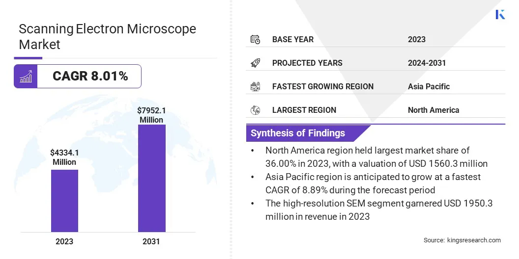
The global scanning electron microscope market size was valued at USD 4,334.1 million in 2023 and is projected to grow from USD 4,637.6 million in 2024 to USD 7,952.1 million by 2031, exhibiting a CAGR of 8.01% during the forecast period.
The market is registering significant growth, fueled by rapid advancements in nanotechnology, increasing adoption across research and industrial applications, and the rising need for high-resolution imaging in material analysis.
The semiconductor industry remains a key driver of the market, utilizing SEMs for defect detection, failure analysis, and process optimization in chip fabrication. The life sciences sector is also expanding its use of SEM technology for cellular and tissue imaging, contributing to breakthroughs in biomedical research and pharmaceutical development.
Major companies operating in the scanning electron microscope industry are Thermo Fisher Scientific Inc., Hitachi High-Tech Corporation, JEOL Group, ZEISS Group, TESCAN GROUP, a.s., Bruker Corporation, ADVANTEST CORPORATION, AMETEK.Inc., Oxford Instruments plc, Angstrom Advanced Inc., Delong America Inc., RAITH GmbH, Nanoscience Instruments, Merck KGaA, and Labtron Equipment Ltd.
Additionally, growing investments in material science, metallurgy, and forensic investigations are bolstering market demand. Government initiatives and funding for academic institutions and research laboratories are further driving SEM adoption, enabling innovation in multiple scientific fields.
The emergence of automated and AI-powered SEMs is enhancing operational efficiency, reducing analysis time, and making the technology more accessible to a broader user base. Furthermore, industries such as automotive, aerospace, and energy are increasingly integrating SEM technology for quality control and failure analysis, reinforcing its importance in manufacturing and product development.
- In April 2024, scientists at the University of Manchester announced the development of AutomaTEM, the world’s first analytical Transmission Electron Microscope (TEM) integrating AI and automated workflows. In collaboration with Thermo Fisher Scientific, the Henry Royce Institute, bp, and EPSRC, the AutomaTEM will enhance high-resolution imaging, spectroscopy, and automation to accelerate materials science research.
Key Highlights:
- The scanning electron microscope industry size was valued at USD 4,334.1 million in 2023.
- The market is projected to grow at a CAGR of 8.01% from 2024 to 2031.
- North America held a market share of 36.00% in 2023, with a valuation of USD 1,560.3 million.
- The high-resolution SEM segment garnered USD 1,950.3 million in revenue in 2023.
- The field emission SEM (FE-SEM) segment is expected to reach USD 3,947.4 million by 2031.
- The material science segment is expected to reach USD 1,951.1 million by 2031.
- The academic & research institutions segment is expected to reach USD 2,391.7 million by 2031.
- The market in Asia Pacific is anticipated to grow at a CAGR of 8.89% during the forecast period.
Market Driver
Advancements in Automation and High-resolution Imaging
The market is registering substantial growth, due to technological advancements, particularly in automation and self-calibration features. Traditional SEMs require skilled operators to manually adjust parameters such as focus, contrast, and electron beam settings, which can be time-consuming and prone to human error.
However, the integration of automation and self-calibration technologies has revolutionized SEM usability by streamlining imaging and analytical workflows. Features such as AI-powered auto-focus, automated contrast adjustments, and real-time calibration enhance efficiency, reduce operator workload, and ensure consistent, high-quality imaging.
These advancements are particularly beneficial in research and industrial applications facing workforce shortages, as they minimize the dependency on highly trained personnel while improving throughput and accuracy.
- In July 2024, JEOL announced the release of the JSM-IT810 Schottky Field Emission Scanning Electron Microscope (FE-SEM), featuring the "Neo Action" automatic observation and analysis function and the "SEM Automatic Adjustment Package" for calibration. This advancement enhances efficiency, productivity, and EDS integration, addressing labor shortages in research and industry.
Market Challenge
High Cost and Accessibility Challenges
A major challenge in the scanning electron microscope (SEM) market is the high cost of acquisition, maintenance, and operation. Advanced SEM systems, especially those with features like multi-modal imaging, and AI-driven automation, require significant investment, often ranging from hundreds of thousands to millions of dollars.
Additionally, operational costs such as regular maintenance, consumables like electron sources, and the need for highly skilled personnel further add to the financial burden. This makes SEM technology less accessible to small research institutions, universities, and emerging industries, limiting its widespread adoption despite its critical role in material science, nanotechnology, and biomedical research.
Manufacturers are shifting toward cost-efficient, compact, and user-friendly SEM solutions. The development of benchtop SEMs with automated calibration, AI-driven image processing, and simplified workflows is lowering the technical expertise required, making these systems more accessible to a broader user base.
Additionally, leasing models, government-backed research funding, and industry-academia collaborations are facilitating broader access to high-end SEM technology.
Market Trend
AI-powered Automation and Multi-modal Hybrid Microscopy
The scanning electron microscope market is registering significant transformation driven by advancements in AI-powered and autonomous microscopy workflows. Traditional SEM imaging and analysis require extensive user expertise; however, recent developments in Artificial Intelligence (AI) and Machine Learning (ML) are enabling automated image acquisition, analysis, and defect detection.
AI-powered SEMs can intelligently adjust imaging parameters, recognize patterns, and enhance resolution in real time, significantly improving efficiency and reproducibility. These autonomous capabilities reduce the burden on skilled operators, making high-precision microscopy more accessible across various industries, including materials science, nanotechnology, and biomedical research.
Another key trend shaping the market is the growing demand for multi-modal and hybrid microscopy solutions. Researchers and industries are increasingly integrating SEM with complementary imaging techniques such as energy-dispersive X-ray spectroscopy (EDS), focused ion beam (FIB), and transmission electron microscopy (TEM) to obtain a more comprehensive understanding of materials at multiple scales.
These hybrid systems enable simultaneous structural, compositional, and chemical analysis, enhancing research capabilities in fields like semiconductor manufacturing, failure analysis, and energy materials development. As a result, manufacturers are focusing on developing versatile, multi-functional SEMs to meet the evolving needs of high-end research and industrial applications.
- In October 2024, Thermo Fisher Scientific introduced the Thermo Scientific Iliad at the European Microscopy Congress, Denmark. This fully integrated multimodal analytical (Scanning) Transmission Electron Microscope combines EELS, NanoPulser electrostatic beam blanker, and Energy Dispersive Spectroscopy (EDS) to provide atomic-level chemical insights. Featuring the Velox software ecosystem and Python-based Autoscript control, Iliad enables AI-driven data collection and advanced microscopy workflows, revolutionizing materials science research.
Scanning Electron Microscope Market Report Snapshot
|
Segmentation
|
Details
|
|
By Resolution Type
|
Standard-Resolution SEM, High-Resolution SEM, Ultra-High-Resolution SEM
|
|
By Type
|
Conventional SEM, Field Emission SEM (FE-SEM), Variable Pressure SEM (VP-SEM)
|
|
By Application
|
Material Science, Life Sciences & Healthcare, Semiconductor & Electronics, Industrial Manufacturing, Others
|
|
By End User
|
Academic & Research Institutions, Industrial & Manufacturing Companies, Semiconductor & Electronics Industry, Healthcare & Life Sciences Organizations, Forensic & Environmental Laboratories
|
|
By Region
|
North America: U.S., Canada, Mexico
|
|
Europe: France, UK, Spain, Germany, Italy, Russia, Rest of Europe
|
|
Asia-Pacific: China, Japan, India, Australia, ASEAN, South Korea, Rest of Asia-Pacific
|
|
Middle East & Africa: Turkey, UAE, Saudi Arabia, South Africa, Rest of Middle East & Africa
|
|
South America: Brazil, Argentina, Rest of South America
|
Market Segmentation:
- By Resolution Type (Standard-Resolution SEM, High-Resolution SEM, Ultra-High-Resolution SEM): The high-resolution SEM segment earned USD 1,950.3 million in 2023, due to its critical role in nanotechnology, semiconductor inspection, and advanced material analysis, driving demand in research and industrial applications.
- By Type (Conventional SEM, Field Emission SEM (FE-SEM), Variable Pressure SEM (VP-SEM)): The field emission SEM (FE-SEM) segment held 45.00% share of the market in 2023, due to its superior imaging capabilities, high resolution, and widespread use in precision applications such as microelectronics, life sciences, and failure analysis.
- By Application (Material Science, Life Sciences & Healthcare, Semiconductor & Electronics, Industrial Manufacturing, and Others): The material science segment is projected to reach USD 1,951.1 million by 2031, owing to the growing need for detailed surface characterization in metallurgy, polymers, and advanced materials research across various industries.
- By End User (Academic & Research Institutions, Industrial & Manufacturing Companies, Semiconductor & Electronics Industry, Healthcare & Life Sciences Organizations, and Forensic & Environmental Laboratories): The academic & research institutions segment is projected to reach USD 2,391.7 million by 2031, owing to increased funding for scientific research, expanding university collaborations, and the rising adoption of SEMs in educational and laboratory settings.
Scanning Electron Microscope Market Regional Analysis
Based on region, the global scanning electron microscope market has been classified into North America, Europe, Asia Pacific, Middle East & Africa, and Latin America.
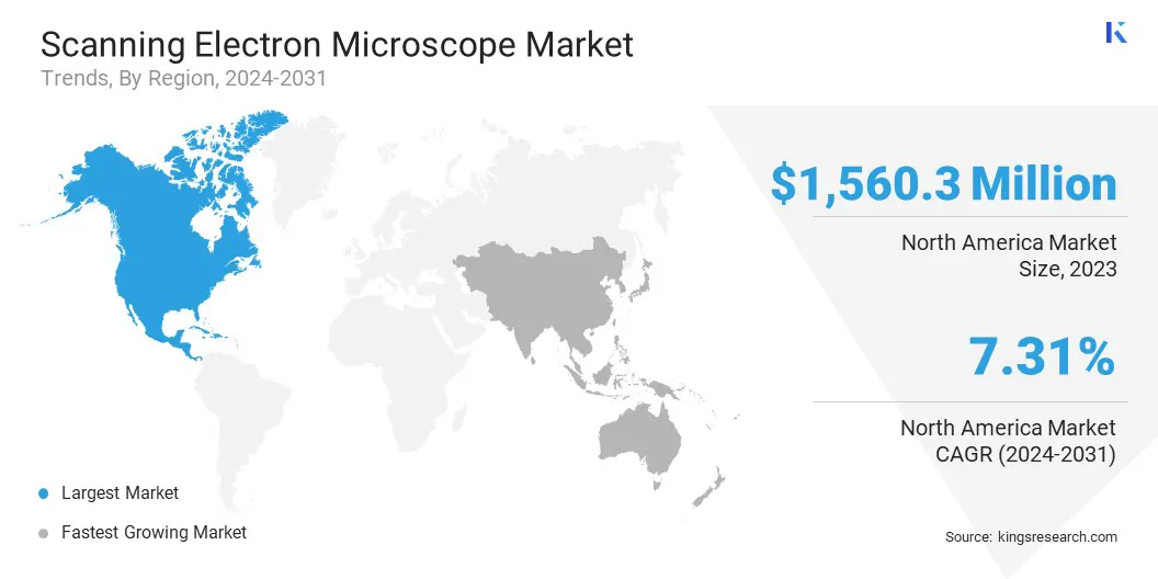
North America accounted for 36.00% share of the scanning electron microscope market in 2023, with a valuation of USD 1,560.3 million. The dominance is driven by increasing investments in semiconductor manufacturing, materials science research, and healthcare applications.
Countries such as China, Japan, South Korea, and India are at the forefront of technological advancements, with strong demand for SEMs in nanotechnology and electronics industries. The region benefits from a robust industrial base, expanding research institutions, and government initiatives supporting scientific innovation.
Additionally, India's growing focus on biotechnology and academic research is expanding the market scope. The market in Asia Pacific is expected to register strong growth, due to increasing R&D activities, strategic partnerships, and government funding, solidifying its position as a key global hub for SEM adoption.
The market in Asia Pacific is poised to grow at a significant CAGR of 8.89% over the forecast period, driven by rapid advancements in semiconductor manufacturing, nanotechnology, and life sciences research. China, Japan, South Korea, and India are key contributors to market expansion.
China leads in semiconductor fabrication and material analysis, while Japan and South Korea specialize in high-resolution SEM technology for electronics and automotive industries. India’s growing focus on biotechnology and academic research further strengthens regional demand.
The presence of leading SEM manufacturers, expanding research institutions, and strategic partnerships enhances market competitiveness. Additionally, government-backed innovation programs and foreign direct investments in advanced manufacturing are fueling the market.
As a result, the market in Asia Pacific is expected to register sustained expansion, reinforcing its leadership in scientific and industrial applications.
Regulatory Frameworks
- In the U.S., the Food and Drug Administration (FDA) regulates SEMs used in medical, pharmaceutical, and life sciences applications. This includes SEMs for diagnostics, biomedical research, and drug development, ensuring compliance with laboratory equipment standards and Good Laboratory Practices (GLP) for accurate and safe analysis.
- In Europe, the European Union (EU) regulates the market by enforcing safety, environmental, and quality standards. Compliance ensures product safety, electromagnetic compatibility, and restricted hazardous substances, allowing manufacturers to sell within the European Economic Area.
Competitive Landscape
The competitive landscape of the scanning electron microscope industry is characterized by continuous technological advancements, strategic collaborations, and increasing investments in Research and Development (R&D). Market players are focused on enhancing imaging capabilities, automation, and AI integration to improve resolution, speed, and user-friendliness.
The market is registering a strong presence of established manufacturers and emerging companies that are innovating to meet the evolving demands of sectors such as semiconductors, life sciences, materials science, and forensics. Additionally, miniaturization and portable SEM models are gaining traction, particularly for field-based research and industrial inspections.
Companies are also investing in hybrid imaging technologies, combining SEM with techniques like energy-dispersive X-ray spectroscopy (EDS) and focused ion beam (FIB) systems to provide comprehensive material characterization solutions. Furthermore, regional expansion strategies are being implemented by key players to strengthen their presence in growing markets where strong investments in semiconductor manufacturing and scientific research are driving demand.
Price differentiation, product customization, and service offerings such as extended warranties, maintenance, and training programs play a crucial role in market competition. Companies are focusing on enhancing imaging performance, affordability, and ease of use to gain a competitive edge in this evolving market as the demand for SEM technology continues to rise across diverse industries.
- In March 2025, Bruker announced the acquisition of Nion, a leader in high-end STEM technology and ultra-high-resolution EELS. This acquisition expands Bruker’s materials science research portfolio and supports advancements in electron diffraction crystallography.
List of Key Companies in Scanning Electron Microscope Market:
- Thermo Fisher Scientific Inc.
- Hitachi High-Tech Corporation
- JEOL Group
- ZEISS Group
- TESCAN GROUP, a.s.
- Bruker Corporation
- ADVANTEST CORPORATION
- AMETEK.Inc.
- Oxford Instruments plc
- Angstrom Advanced Inc.
- Delong America Inc.
- RAITH GmbH
- Nanoscience Instruments
- Merck KGaA
- Labtron Equipment Ltd
Recent Developments (Partnerships/New Product Launch)
- In October 2024, ZEISS launched the Crossbeam 550 Samplefab, an automated FIB-SEM for high-throughput TEM sample preparation. It enables hands-free lamella production with >90% automation yield, a new user-friendly interface, and minimal operator intervention, enhancing semiconductor defect analysis.
- In July 2024, Shimadzu Corporation announced a business partnership agreement with TESCAN GROUP. a.s., a leading SEM manufacturer based in the Czech Republic. As part of this collaboration, TESCAN's SEMs will be added to Shimadzu's analytical measurement product lineup and launched in Japan in autumn 2024.
- In July 2023, JEOL Ltd. introduced the JSM-IT210 InTouchScope and JSM-IT710HR SEMs at M&M 2023. These next-generation SEMs feature advanced automation, Live EDS analysis, Live 3D microscopy, and ZeroMag software for high-resolution imaging and fast data acquisition. The JSM-IT710HR is a Schottky Field Emission SEM for precision imaging, while the JSM-IT210 InTouchScope offers an intuitive, automated workflow for seamless analysis.


