Market Definition
The market encompasses machinery and technologies used in semiconductor fabrication, enabling precise patterning of microcircuits on silicon wafers.
It includes photolithography, extreme ultraviolet (EUV), deep ultraviolet (DUV), and nanoimprint lithography systems. The report outlines the major factors driving the market, along with key drivers and the competitive landscape shaping the growth trajectory over the forecast period.
Lithography Equipment Market Overview
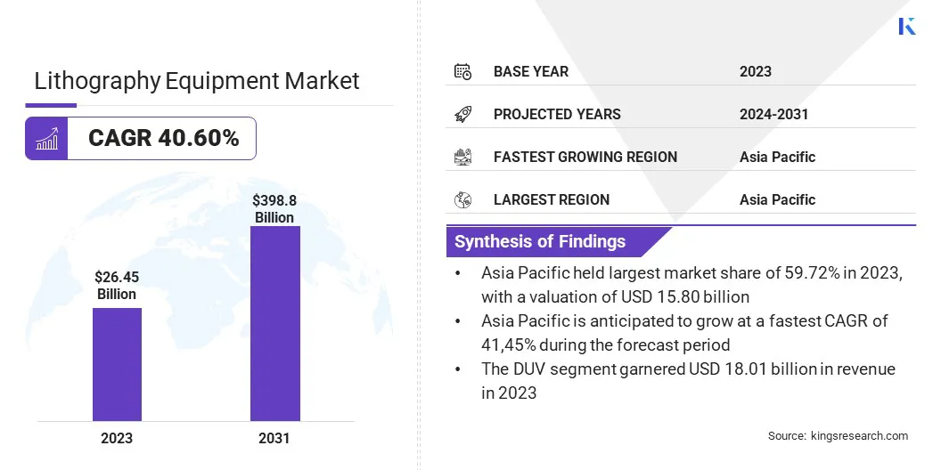
The global lithography equipment market size was valued at USD 26.45 billion in 2023 and is projected to grow from USD 36.71 billion in 2024 to USD 398.8 billion by 2031, exhibiting a CAGR of 40.60% during the forecast period.
This market is expanding rapidly, driven by the increasing need for advanced semiconductor chips across industries like consumer electronics, AI, automotive, and telecommunications.
The rollout of 5G networks fuels the need for high-speed, low-latency chips, while AI and high-performance computing need smaller, more powerful semiconductors, boosting the adoption of EUV lithography. The rising popularity of Electric Vehicles (EVs) and autonomous driving technologies is generating the need for advanced semiconductor components, necessitating cutting-edge lithography processes.
Major companies operating in the lithography equipment industry are ASML, Nikon Corporation, Canon Inc., Applied Materials, Inc., LAM RESEARCH CORPORATION, SUSS MicroTec SE, EV Group, JEOL Group, KLA Corporation, Veeco Instruments Inc., RAITH GmbH, Mycronic, SCREEN Semiconductor Solutions Co., Ltd., Neutronix Quintel, and Onto Innovation.
The shift toward advanced packaging techniques, such as chiplet architecture and 3D stacking, requires more precise lithography solutions to improve performance and efficiency.
The increasing focus on energy-efficient and high-performance computing solutions in data centers also contributes to market growth, as companies seek lithography technologies that enable higher transistor density with lower power consumption. These factors drive innovation and investment in next-generation lithography equipment, ensuring sustained market expansion.
- In September 2024, Canon Inc. supplied its FPA-1200NZ2C Nanoimprint Lithography (NIL) system for semiconductor manufacturing to the Texas Institute for Electronics (TIE). This system, which utilizes NIL technology instead of conventional projection exposure, enables high-precision patterning with reduced power consumption and cost. The equipment will support semiconductor research, development, and prototyping at TIE, reinforcing Canon's commitment to advancing semiconductor manufacturing technology.
Key Highlights:
- The lithography equipment industry size was valued at USD 26.45 billion in 2023.
- The market is projected to grow at a CAGR of 40.60% from 2024 to 2031.
- Asia Pacific held a market share of 59.72% in 2023, with a valuation of USD 15.80 billion.
- The DUV segment garnered USD 18.01 billion in revenue in 2023.
- The ArF immersion segment is expected to reach USD 159.57 billion by 2031.
- The advanced packaging segment is expected to reach USD 167.98 billion by 2031.
- The 3d IC segment is expected to reach USD 157.78 billion by 2031.
- The market in North America is anticipated to grow at a CAGR of 40.51% during the forecast period.
Market Driver
High-NA EUV Advancements and Growing Semiconductor Demand
The market is driven by continuous advancements in High-Numerical Aperture (NA) EUV lithography and the increasing demand for miniaturization and power-efficient semiconductor devices.
High-NA EUV lithography is a major breakthrough, allowing chipmakers to achieve higher precision and transistor density by enabling finer patterning and reducing feature sizes. This enhances chip performance, which is essential for applications requiring high computational efficiency, such as Artificial Intelligence (AI) and high-performance computing.
- In January 2024, ZEISS Semiconductor Manufacturing Technology and ASML delivered the first High-NA EUV lithography system, marking a breakthrough in semiconductor manufacturing. The technology, developed by ZEISS in collaboration with ASML and European partners, enables three times higher transistor density on microchips, significantly enhancing computing power. The optical system, consisting of over 40,000 precision-engineered parts, allows for EUV light exposure with nanometer accuracy.
Additionally, industries are developing more compact and powerful electronics, pushing the need for miniaturization and energy efficiency in semiconductor devices. Consumer electronics, IoT devices, and AI-driven applications demand smaller chips with superior performance, compelling semiconductor manufacturers to adopt cutting-edge lithography solutions for sub-2nm process nodes.
Market Challenge
High Costs and Complexity
A major challenge in the lithography equipment market is the high cost and complexity associated with advanced lithography technologies, particularly high-NA EUV systems. The development and deployment of these cutting-edge tools require billions of dollars in investment, due to their intricate optics, precision engineering, and extreme manufacturing conditions.
Additionally, the operational costs of maintaining and calibrating these systems add to the financial burden on semiconductor manufacturers. This makes it difficult for smaller foundries and emerging players to compete, limiting access to next-generation chip fabrication.
Semiconductor manufacturers and equipment suppliers are increasingly adopting cost-sharing models, industry collaborations, and government-backed initiatives to distribute the financial burden. Companies are also focusing on optimizing process efficiency, extending the lifespan of existing lithography tools, and integrating AI-driven automation to enhance productivity while reducing costs.
Market Trend
Maskless Lithography and Panel-level Packaging
The market is evolving with the emergence of maskless lithography and the growing adoption of Panel-level Packaging (PLP) in semiconductor manufacturing.
Maskless lithography eliminates the need for physical photomasks by using digital projection techniques or direct-write methods, significantly reducing production time and mask-related costs while enhancing design flexibility. This enables rapid prototyping and customization, making it ideal for next-generation chip architectures.
Simultaneously, panel-level packaging is optimizing semiconductor fabrication by increasing efficiency and yield. Unlike traditional wafer-level packaging, which is limited by circular wafer sizes, PLP uses larger, rectangular substrates, allowing multiple chips to be processed simultaneously with improved material utilization.
This approach reduces waste, lowers costs, and enhances the electrical performance of semiconductor devices, meeting the growing need for high-performance and cost-efficient chips in AI, IoT, and high-speed computing applications.
- In October 2024, Nikon Corporation announced the development of a digital lithography system with 1.0-micron (L/S) resolution for advanced semiconductor packaging applications. The system eliminates the need for photomasks, reducing costs and production time. Nikon aims to enhance high-resolution exposure for panel-level packaging by integrating multi-lens technology from its FPD lithography systems, supporting the growing demand for AI-driven semiconductor manufacturing.
Lithography Equipment Market Report Snapshot
|
Segmentation
|
Details
|
|
By Type
|
EUV, DUV
|
|
By Technology
|
ArF Scanners, KrF Steppers, I-line Steppers, ArF Immersion, Mask Aligners, Others
|
|
By Applications
|
Advanced Packaging, LED, MEMs, Power Devices
|
|
By Packaging Platforms
|
3D IC, 2.5D Interposer, Wafer Level Chip Scale Packaging (WLCSP), FO WLP Wafer, 3D WLP, Others
|
|
By Region
|
North America: U.S., Canada, Mexico
|
|
Europe: France, UK, Spain, Germany, Italy, Russia, Rest of Europe
|
|
Asia-Pacific: China, Japan, India, Australia, ASEAN, South Korea, Rest of Asia-Pacific
|
|
Middle East & Africa: Turkey, UAE, Saudi Arabia, South Africa, Rest of Middle East & Africa
|
|
South America: Brazil, Argentina, Rest of South America
|
Market Segmentation
- By Type (EUV, DUV): The DUV segment earned USD 18.01 billion in 2023, due to its widespread use in mature semiconductor nodes and cost-effectiveness compared to EUV for various chip applications.
- By Technology (ArF Scanners, KrF Steppers, I-line Steppers, ArF Immersion, Mask Aligners, Others): The ArF immersion segment held 38.74% share of the market in 2023, due to its ability to achieve high-resolution patterning for advanced semiconductor nodes, making it essential for leading-edge chip manufacturing.
- By Applications (Advanced Packaging, LED, MEMs, and Power Devices): The advanced packaging segment is projected to reach USD 167.98 billion by 2031, owing to the growing need for high-performance computing and heterogeneous integration in semiconductor design.
- By Packaging Platforms (3D IC, 2.5D Interposer, Wafer Level Chip Scale Packaging (WLCSP), FO WLP Wafer, 3D WLP, Others): The 3d IC segment is projected to reach USD 157.78 billion by 2031, owing to its ability to enhance chip performance, reduce power consumption, and enable higher transistor density in compact devices.
Lithography Equipment Market Regional Analysis
Based on region, the market has been classified into North America, Europe, Asia Pacific, Middle East & Africa, and Latin America.
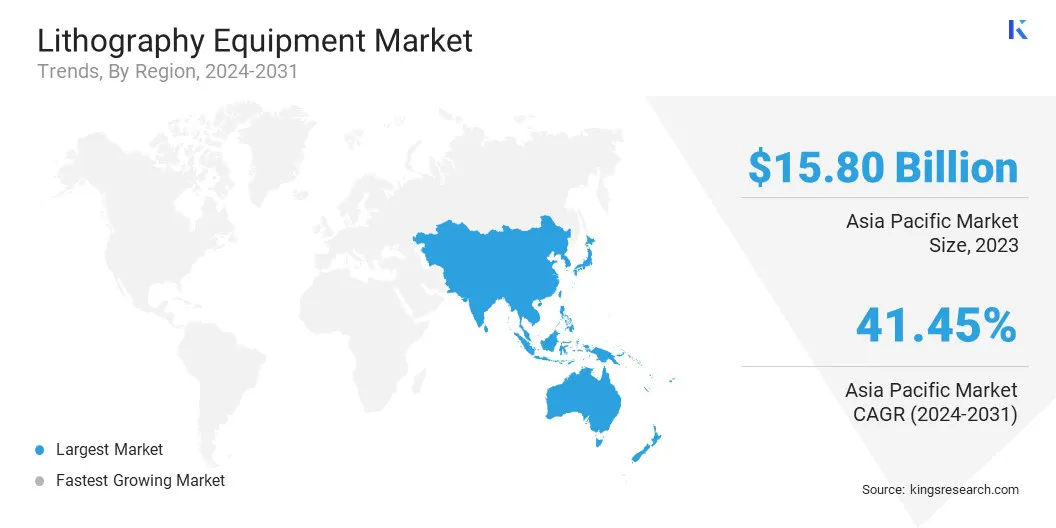
Asia Pacific accounted for 36.42% share of the lithography equipment market in 2023, with a valuation of USD 15.80 billion. The market in the region is driven by the dominance of semiconductor manufacturing hubs such as Taiwan, South Korea, China, and Japan.
Taiwan Semiconductor Manufacturing Company (TSMC) and South Korea's Samsung Electronics lead in advanced node production, heavily investing in EUV and DUV lithography equipment to maintain technological leadership. The presence of key semiconductor foundries, coupled with continuous technological advancements in fabrication processes, has fueled regional growth.
Additionally, China's increasing investments in domestic semiconductor firms and Japan’s strong position in photolithography materials, such as photoresists and mask blanks, contribute to the region's leadership in the market.
- In December 2024, Rapidus Corporation installed ASML's NXE:3800E EUV lithography equipment at its IIM-1 foundry in Japan. This marks the first EUV lithography system for mass production in Japan, enabling 2nm semiconductor fabrication using advanced optical systems and reflective photomasks. The installation supports Rapidus' goal of establishing a pilot production line by April 2025.
The lithography equipment industry in North America is expected to register the fastest growth in the market, with a projected CAGR of 40.51% over the forecast period. This expansion is driven by significant investments from leading semiconductor manufacturers such as Intel, GlobalFoundries, and Texas Instruments in advanced chip production.
The region benefits from a well-established ecosystem of semiconductor research institutions and technology collaborations, fostering continuous innovation in lithography processes. The increasing focus on AI, quantum computing, and high-performance computing is accelerating the need for next-generation chips, requiring more sophisticated lithography solutions.
Additionally, North America's strong expertise in developing advanced chip architectures, including chiplet-based designs and heterogeneous integration, is further boosting the need for high-precision lithography equipment.
North America is poised to emerge as a critical hub for lithography technology advancements, due to the growing emphasis on self-reliant semiconductor supply chains and the expansion of cutting-edge fabrication facilities.
Regulatory Frameworks
- In the U.S., the Bureau of Industry and Security (BIS) enforces export controls on advanced lithography equipment, particularly EUV systems, to restrict technology transfers to certain countries. The Environmental Protection Agency (EPA) regulates the use of hazardous chemicals in lithography processes, while the Semiconductor Equipment and Materials International (SEMI) sets industry standards for manufacturing precision and efficiency.
- In the European Union (EU), the European Chemicals Agency (ECHA) enforces REACH regulations, restricting hazardous chemicals used in lithography processes, while the European Commission (EC) monitors semiconductor trade policies and promotes local semiconductor manufacturing initiatives.
- In China, the Ministry of Industry and Information Technology (MIIT) oversees policies supporting domestic semiconductor equipment development, while the China National Intellectual Property Administration (CNIPA) regulates intellectual property rights related to lithography technologies.
- In Japan, the Ministry of Economy, Trade, and Industry (METI) controls export restrictions on advanced semiconductor manufacturing equipment, while Japan Industrial Standards (JIS) set precision and efficiency guidelines for lithography systems.
Competitive Landscape
The lithography equipment market is characterized by key players focusing on technological innovation, strategic partnerships, and capacity expansion to maintain market leadership.
Companies are heavily investing in research and development to enhance resolution capabilities, improve throughput, and enable cost-effective chip manufacturing at smaller nodes. The adoption of EUV lithography is a primary focus, with firms working on refining EUV source power and pellicle technology to improve efficiency.
Major lithography equipment manufacturers are forming alliances with semiconductor foundries and integrated device manufacturers (IDMs) to co-develop next-generation fabrication techniques. Some players are expanding their production facilities and optimizing supply chains to meet the rising global need for advanced semiconductor manufacturing tools.
Additionally, firms are focusing on extending the lifespan and efficiency of existing lithography systems by developing advanced upgrade kits and modular enhancements, allowing semiconductor manufacturers to optimize performance without investing in entirely new equipment.
The emphasis on enhancing overlay accuracy and reducing patterning variability through novel optical and computational lithography techniques is growing, enabling better yield control in advanced node production.
- In December 2023, Applied Materials, Inc. and Ushio, Inc. announced a strategic partnership to accelerate the industry’s transition to heterogeneous chiplet integration for advanced semiconductor packaging. The collaboration introduces a new Digital Lithography Technology (DLT) system designed to pattern high-density interconnects on large substrates such as glass and organic materials, enabling advanced AI-era computing with sub-micron wiring precision.
List of Key Companies in Lithography Equipment Market:
Recent Developments (Acquisition/Partnerships/Product Launches)
- In March 2025, imec and ZEISS Semiconductor Manufacturing Technology signed a Strategic Partnership Agreement to extend their collaboration until 2029. The partnership focuses on advancing high-NA EUV lithography and sub-2nm semiconductor research through imec’s NanoIC pilot line. ZEISS will contribute lithography optics and support research projects, reinforcing Europe's leadership in semiconductor manufacturing in alignment with the European Chips Act.
- In December 2024, ZEISS Semiconductor Manufacturing Technology successfully acquired the Lithography division of Beyond Gravity. The acquisition expands ZEISS’s production and R&D capacities to meet the growing need for semiconductor manufacturing systems.
- In May 2024, Canon Inc. announced the launch of the new Flat Panel Display (FPD) lithography system compatible with 6th generation substrates. The system enhances display manufacturing efficiency by offering wider exposure, improved overlay accuracy, and higher productivity. It reduces the number of exposure shots required for smartphone and automotive displays, enabling cost-effective mass production of high-resolution, thin, and lightweight displays.
- In April 2024, Intel Foundry installed and began calibrating the industry's first high-NA EUV lithography system, developed by ASML. This advanced tool, housed at Intel's D1X factory in Oregon, enhances chip manufacturing, enabling higher resolution and feature scaling for next-generation processors.


