Market Definition
The 3D stacking process integrates multiple semiconductor layers into a single package to enhance device performance and reduce footprint. It combines advanced interconnecting technologies such as 3D hybrid bonding, through-silicon vias, and monolithic 3D integration to achieve higher speed, efficiency, and density.
This process is applied in devices such as memory, logic ICs, imaging components, LEDs, and MEMS sensors, enabling diverse functionality. It serves industries such as consumer electronics, communications, automotive, manufacturing, and healthcare, supporting compact designs, improved performance, and efficient system integration.
3D Stacking Market Overview
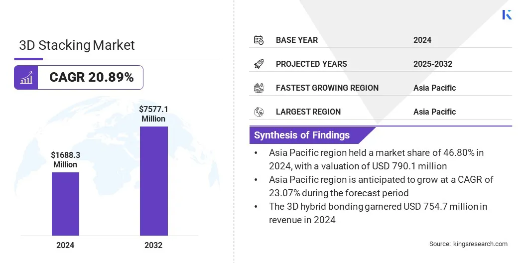
The global 3D stacking market size was valued at USD 1,688.3 million in 2024 and is projected to grow from USD 2,008.3 million in 2025 to USD 7,577.1 million by 2032, exhibiting a CAGR of 20.89% over the forecast period.
The growth is driven by the increasing demand for next-generation custom accelerators, which require high-performance and energy-efficient semiconductor solutions. Advancements in layer transfer technology, such as shifting ultra-thin transistor layers onto diverse wafers for heterogeneous integration, are improving interconnect density and device performance.
Key Highlights:
- The 3D stacking industry size was recorded at USD 1,688.3 million in 2024.
- The market is projected to grow at a CAGR of 20.89% from 2025 to 2032.
- Asia Pacific held a market share of 46.80% in 2024, with a valuation of USD 790.1 million.
- The chip-to-chip segment garnered USD 499.7 million in revenue in 2024.
- The 3D hybrid bonding segment is expected to reach USD 4,361.2 million by 2032.
- The memory devices segment is expected to reach USD 2,775.3 million by 2032.
- The consumer electronics segment is expected to reach USD 2,051.8 million by 2032.
- North America is anticipated to grow at a CAGR of 19.68% over the forecast period.
Major companies operating in the 3D stacking market are Taiwan Semiconductor Manufacturing Company Limited, Intel Corporation, Samsung, Advanced Micro Devices, Inc., SK HYNIX INC., ASE, Amkor Technology, Powertech Technology Inc., Jiangsu Changdian Technology Co., Ltd., XMC, Tezzaron, BroadPak Corporation, X-FAB Silicon Foundries SE, United Microelectronics Corporation, and Texas Instruments Incorporated.
Market growth is propelled by the adoption of advanced multi-die packaging for AI accelerators, which enables the integration of multiple high-performance chips within a single package. This improves processing speed, reduces latency, and enhances energy efficiency for AI and machine learning workloads.
Manufacturers are leveraging innovative interconnects and thermal management solutions to optimize performance and reliability in densely packed architectures. The technology supports scalable and flexible designs, allowing companies to meet the increasing computational demands of next-generation AI applications.
- In May 2025, Marvell Technology, Inc. launched a new multi-die packaging platform designed for custom AI accelerators. The platform allows larger multi-chip configurations while reducing power consumption and overall costs, and it improves die-to-die interconnect efficiency. It incorporates a modular RDL interposer as an alternative to conventional silicon interposers and supports HBM3/3E memory integration.
Market Driver
Growing Demand for Next-Generation Custom Accelerators
The 3D stacking market is driven by the growing demand for next-generation custom accelerators, which are essential for high-performance computing, artificial intelligence, and data center applications. 3D stacking enables high-speed processing and energy efficiency by integrating multiple semiconductor layers within a single package, meeting the performance needs of modern accelerators.
This allows manufacturers to achieve higher computational power and reduced latency while maintaining a compact footprint. The demand for enhanced performance in specialized computing applications is accelerating the adoption of 3D stacking technologies across various industries.
- In December 2024, Broadcom Inc. introduced its 3.5D eXtreme Dimension System in Package (XDSiP) platform to support custom AI XPUs. The platform merges 3D silicon stacking with 2.5D packaging, enabling the integration of multiple compute dies, I/O dies, and HBM memory stacks in a single package. It improves interconnect density, lowers power consumption, and reduces latency, while maintaining a compact package design for AI applications.
Market Challenge
Thermal Management Issues in 3D Stacking Devices
A major challenge in the 3D Stacking market is managing heat dissipation in high-density stacked chips. Increased layer density generates more heat, which can reduce device performance and reliability. This limits widespread adoption, especially in high-performance computing and compact electronic devices.
To address this, companies are investing in advanced thermal management solutions, including microfluidic cooling and improved heat-spreading materials. Manufacturers are also optimizing chip architecture and stacking designs to enhance heat dissipation and maintain consistent performance.
Market Trend
Advancements in Layer Transfer Technology
A key trend in the 3D stacking market is the use of ultra-thin transistor layer transfers onto diverse wafers, enabled by advancements in heterogeneous integration. This allows manufacturers to stack diverse semiconductor layers efficiently, improving interconnect density and signal integrity.
It also enables the combination of logic, memory, and specialized chips within a single package, enhancing overall device performance. Companies are adopting this technique to meet the growing demand for compact, high-performance, and energy-efficient electronic devices.
- In June 2025, Soitec and Powerchip Semiconductor Manufacturing Corporation (PSMC) announced a strategic collaboration to advance ultra-thin Transistor Layer Transfer (TLT) technology for nm-scale 3D stacking. The partnership focuses on supplying 300mm substrates with a release layer to enable high-speed transfer of ultra-thin transistor layers and support next-generation 3D chip stacking.
3D Stacking Market Report Snapshot
|
Segmentation
|
Details
|
|
By Method
|
Chip-to-Chip, Chip-to-Wafer, Die-to-Die, Die-to-Wafer, Wafer-to-Wafer
|
|
By Interconnecting Technology
|
3D Hybrid Bonding, 3D TSV (Through-Silicon Via), Monolithic 3D Integration
|
|
By Device Type
|
Memory Devices, Logic ICs, Imaging & Optoelectronics, LEDs, MEMS/ Sensors, Others
|
|
By End-Use Industry
|
Consumer Electronics, Communications, Automotive, Manufacturing, Medical Devices & Healthcare, Others
|
|
By Region
|
North America: U.S., Canada, Mexico
|
|
Europe: France, UK, Spain, Germany, Italy, Russia, Rest of Europe
|
|
Asia-Pacific: China, Japan, India, Australia, ASEAN, South Korea, Rest of Asia-Pacific
|
|
Middle East & Africa: Turkey, U.A.E., Saudi Arabia, South Africa, Rest of Middle East & Africa
|
|
South America: Brazil, Argentina, Rest of South America
|
Market Segmentation:
- By Method (Chip-to-Chip, Chip-to-Wafer, Die-to-Die, Die-to-Wafer, and Wafer-to-Wafer): The chip-to-chip segment earned USD 499.7 million in 2024, due to high adoption in compact and high-performance electronic devices.
- By Interconnecting Technology (3D Hybrid Bonding, 3D TSV (Through-Silicon Via), and Monolithic 3D Integration): The 3D hybrid bonding segment held 44.70% of the market in 2024, due to its higher interconnect density and improved signal performance.
- By Device Type (Memory Devices, Logic ICs, Imaging & Optoelectronics, LEDs, MEMS/ Sensors, and Others) : The memory devices segment is projected to reach USD 2,775.3 million by 2032, owing to rising demand for high-capacity and energy-efficient storage solutions.
- By End-Use Industry (Consumer Electronics, Communications, Automotive, Manufacturing, Medical Devices & Healthcare, and Others) : The consumer electronics segment is projected to reach USD 2,051.8 million by 2032, owing to the increasing integration of advanced semiconductors in smartphones and wearables.
3D Stacking Market Regional Analysis
Based on region, the market has been classified into North America, Europe, Asia Pacific, Middle East & Africa, and South America.
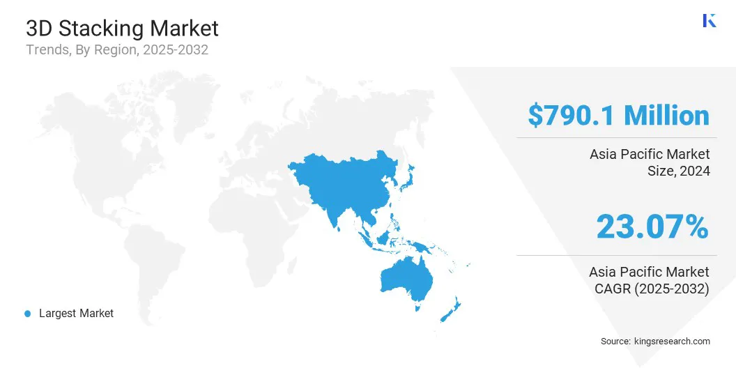
Asia Pacific 3D stacking market share stood at 46.80% in 2024 in the global market, with a valuation of USD 790.1 million. This dominance is due to the presence of large-scale semiconductor manufacturing hubs and high adoption of advanced packaging technologies in countries such as China, Japan, and South Korea.
Semiconductor companies in the region benefit from cost-efficient production, a skilled workforce, and government support for semiconductor infrastructure, driving the broader adoption of 3D stacking solutions.
North America is poised to grow at a CAGR of 19.68% over the forecast period. This growth is driven by strong R&D efforts focused on innovative materials and advanced 3D stacking techniques. Semiconductor companies in the region utilize research facilities and strategic partnerships to improve chip efficiency and density, accelerating adoption in consumer electronics, automotive, and communication sectors.
- In April 2025, MIT Lincoln Laboratory developed a specialized benchmarking chip to test cooling solutions for 3D integrated microelectronics. The chip generates high power to simulate heat in stacked circuits and measures temperature changes as cooling methods are applied. The project, funded by DARPA under the Minitherms3D program, supports HRL Laboratories in developing thermal management systems for 3D heterogeneous integrated stacks.
Regulatory Frameworks
- In the U.S, the Bureau of Industry and Security (BIS) regulates 3D stacking technologies by controlling exports of advanced semiconductor manufacturing equipment and restricting transfers to foreign entities.
- In Europe, the European Commission regulates through the European Chips Act, which sets rules for investment, manufacturing, and innovation incentives, ensuring secure and resilient semiconductor supply chains.
- In Japan, the Ministry of Economy, Trade and Industry regulates 3D chiplet development by supporting research programs, setting industry standards, and offering incentives to domestic semiconductor manufacturers.
Competitive Landscape
Key players in the global 3D stacking industry are focusing on enhancing device performance and efficiency through advanced material innovations. Companies are investing in research to develop new materials that reduce chip capacitance, which improves signal integrity and lowers power consumption in stacked logic and DRAM chips.
Manufacturers are implementing complex thermal management solutions to maintain performance stability in high-density 3D structures. Moreover, market players are pursuing strategic collaborations with equipment suppliers and research institutions to accelerate the adoption of these materials and optimize the 3D stacking process for high-performance applications.
- In July 2024, Applied Materials, Inc. launched new materials engineering solutions to extend copper chip wiring to the 2nm node and beyond. The solution combines ruthenium and cobalt to reduce electrical resistance by up to 25 percent and introduces an enhanced low-k dielectric that strengthens logic and DRAM chips for advanced 3D stacking. This is expected to offer highly energy-efficient computing and improved chip performance.
Key Companies in 3D Stacking Market:
- Taiwan Semiconductor Manufacturing Company Limited
- Intel Corporation
- Samsung
- Advanced Micro Devices, Inc.
- SK HYNIX INC.
- ASE
- Amkor Technology
- Powertech Technology Inc.
- Jiangsu Changdian Technology Co., Ltd.
- XMC
- Tezzaron
- BroadPak Corporation
- X-FAB Silicon Foundries SE
- United Microelectronics Corporation
- Texas Instruments Incorporated
Recent Developments (Partnerships/New Product Launch)
- In August 2025, Socionext Inc. expanded its portfolio with advanced 3DIC solutions, including enhanced 3D die stacking and 5.5D packaging technologies. The offering features face-to-face (F2F) 3D stacking of N3 compute and N5 I/O dies, enabling higher integration density, lower power consumption, and improved performance for consumer, AI, and HPC applications.
- In June 2024, Ansys announced its integration with NVIDIA Omniverse to enable 3D multiphysics visualization for next-generation 3D-IC designs. The collaboration allows designers to interact with electromagnetic and thermal models in real time, improving diagnostics and optimization for applications including 5G/6G, AI/ML, IoT, and autonomous vehicles. This solution supports multi-die chip stacks, helping optimize performance, reliability, and power efficiency in compact semiconductor packages.
significant


