Market Definition
The market refers to the industry focused on advanced packaging technologies that vertically stack multiple semiconductor components such as chips, dies, or wafers to enhance performance, reduce power consumption, and minimize footprint.
This market includes solutions like Through-Silicon Via (TSV), interposers, and die-stacking techniques, catering to high-demand applications in AI, 5G, IoT, and consumer electronics. They enable higher density, faster speeds, and enhanced functionality in semiconductor devices.
The report outlines the primary drivers of market growth, along with an in-depth analysis of emerging trends and evolving regulatory frameworks shaping the industry's trajectory.
3D Semiconductor Packaging Market Overview
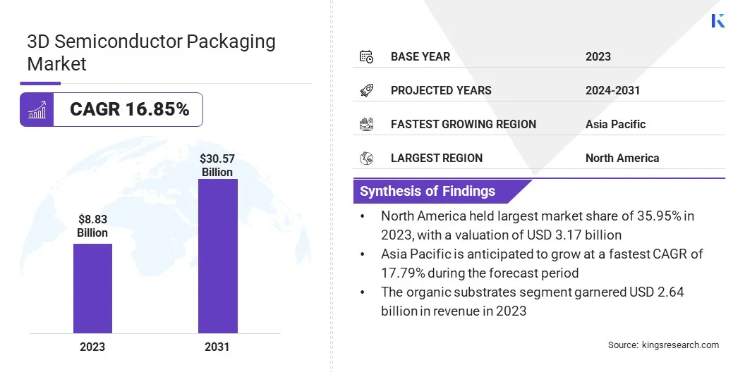
The global 3D semiconductor packaging market size was valued at USD 8.83 billion in 2023 and is projected to grow from USD 10.28 billion in 2024 to USD 30.57 billion by 2031, exhibiting a CAGR of 16.85% during the forecast period.
The market grows with rising demand for compact, high-performance electronics. Vertical stacking enables greater integration without increasing device size, while advanced stacking and design methods support efficient, scalable solutions for edge AI, IoT, and complex computing needs.
Major companies operating in the 3D semiconductor packaging industry are Samsung, Taiwan Semiconductor Manufacturing Company Limited, Intel Corporation, National Institute for Automotive Service Excellence (ASE), Amkor Technology, United Microelectronics Corporation, JCET Group, Powertech Technology Inc., GlobalFoundries (GF), Micron Technology Inc., STMicroelectronics, SUSS MicroTec SE, Tokyo Electron Limited, Broadcom, and Texas Instruments Incorporated.
The market is driven by the rapid expansion of 5G networks, which require advanced packaging solutions to support high-speed, low-latency chip performance. The growing demand for faster data transmission, higher bandwidth, and compact device designs in 5G infrastructure is driving the adoption of 3D packaging. By enabling vertical chip integration, this technology minimizes signal loss and enhances power efficiency.
- In March 2025, The Indian Ministry of Communications, reported that over 25 crore mobile users adopting 5G and 469 thousand 5G BTSs deployed across 99.6% of India’s districts, the rapid expansion of 5G infrastructure is driving strong demand for high-performance semiconductor solutions. This growth directly supports the 3D semiconductor packaging industry, which enables compact, low-latency, and energy-efficient chip integration essential for powering advanced 5G devices, base stations, and edge computing across India’s 971.5 million internet users.
Key Highlights
- The 3D semiconductor packaging market size was recorded at USD 8.83 billion in 2023.
- The market is projected to grow at a CAGR of 16.85% from 2024 to 2031.
- North America held a market share of 35.95% in 2023, with a valuation of USD 3.17 billion.
- The 3D through silicon via segment garnered USD 2.41 billion in revenue in 2023.
- The organic substrates segment is expected to reach USD 9.15 billion by 2031.
- The consumer electronics segment is anticipated to witness fastest CAGR of 17.23% during the forecast period
- Asia Pacific is anticipated to grow at a CAGR of 17.79% during the forecast period.
Market Driver
Miniaturization of Electronic Devices
The 3D semiconductor packaging market is driven by the miniaturization of electronic devices, which require compact, lightweight, and high-performance solutions. With the continued reduction in the size of consumer electronics, wearables, and IoT devices, the demand for increased functionality within constrained physical space continues to rise.
3D packaging enables vertical stacking of components, allowing greater integration and performance without expanding the device footprint, making it a vital technology for modern, space-constrained electronic applications.
- In September 2023, TSMC introduced 3Dblox 2.0, enhancing early-stage 3D IC design with tools for power and thermal analysis in a unified environment. This advancement streamlines the development of complex 3D architectures, facilitates chiplet reuse across multiple designs, and significantly improves design efficiency and scalability. It also supports faster time-to-market by enabling more accurate simulations and reducing the need for iterative physical prototyping.
Market Challenge
Thermal Management Related Issues
Thermal issues from stacked density remain a major challenge in 3D semiconductor packaging. Vertical integration of multiple chips restricts heat dissipation, resulting in elevated power density and localized thermal accumulation.
This can degrade performance and reliability, especially in high-performance computing and mobile devices. To address this, companies are investing in advanced thermal interface materials, integrated heat spreaders, and vapor chambers. Some are also using chiplet architectures to distribute heat more effectively.
Additionally, thermal simulation tools are being used during the design phase to predict and manage heat flow. These strategies help maintain performance while ensuring long-term device stability.
Market Trend
Technological Advancements in 3D Integration
The market is being shaped by technological advancements that enable the integration of memory and processing units through wafer-to-wafer stacking. These innovations address the demand for efficient and high-performance solutions in edge AI applications such as smart infrastructure and the Internet of Things (IoT).
Improvements in system-level verification, design flows, and stacking methods are resolving integration challenges, resulting in scalable, reliable, and power-efficient 3D IC solutions that support the increasing complexity of modern computing environments.
- In October 2023, United Microelectronics Corporation (UMC) launched the W2W (wafer-to-wafer) 3D Integrated Circuit (IC) project in collaboration with Winbond, Faraday, ASE, and Cadence. This initiative aims to accelerate the production of 3D products, offering an integrated solution for memory and processor silicon stacking.
3D Semiconductor Packaging Market Report Snapshot
|
Segmentation
|
Details
|
|
By Technology
|
3D through silicon via, 3D package on package, 3D Wafer-Level Chip-Scale Packaging (WL-CSP), 3D System-On-Chip (3D SoC), 3D Integrated Circuit (3D IC)
|
|
By Material
|
Organic substrates, Bonding wires, Lead frames, Ceramic packages, Encapsulation resins, Others
|
|
By End-use Industry
|
Consumer Electronics, Automotive, Healthcare, IT & Telecommunications, Industrial, Aerospace &Defense, Others
|
|
By Region
|
North America: U.S., Canada, Mexico
|
|
Europe: France, UK, Spain, Germany, Italy, Russia, Rest of Europe
|
|
Asia-Pacific: China, Japan, India, Australia, ASEAN, South Korea, Rest of Asia-Pacific
|
|
Middle East & Africa: Turkey, U.A.E., Saudi Arabia, South Africa, Rest of Middle East & Africa
|
|
South America: Brazil, Argentina, Rest of South America
|
Market Segmentation:
- By Technology (3D through silicon via, 3D package on package, 3D Wafer-Level Chip-Scale Packaging (WL-CSP), 3D System-On-Chip (3D SoC), and 3D Integrated Circuit (3D IC)): The 3D through silicon via segment earned USD 2.41 billion in 2023 due to its ability to enable high-density integration, faster data transfer, and improved performance for advanced computing and communication applications.
- By Material (Organic substrates, bonding wires, Lead frames, and Ceramic packages): The organic substrates held 29.90% of the market in 2023, due to their cost-effectiveness, design flexibility, and widespread use in high-volume consumer electronics requiring lightweight and compact packaging solutions.
- By End-use Industry (Consumer Electronics, Automotive, Healthcare, IT & Telecommunications, Industrial, Aerospace & Defense, Others): The healthcare segment is projected to reach USD 7.68 billion by 2031, due to the rising adoption of advanced medical devices and wearable technologies that require compact, high-performance, and energy-efficient semiconductor packaging solutions.
3D Semiconductor Packaging Market Regional Analysis
Based on region, the global market has been classified into North America, Europe, Asia Pacific, Middle East & Africa, and South America.
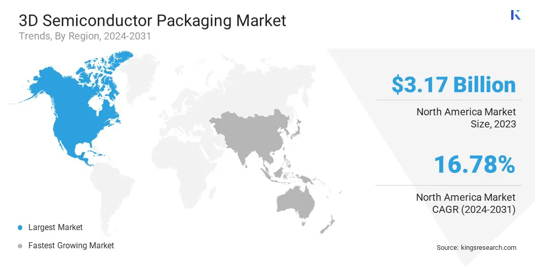
North America 3D semiconductor packaging market share stood at around 35.95% in 2023 in the global market, with a valuation of USD 3.17 billion. North America's dominance in the market is driven by significant investments in advanced manufacturing infrastructure and the growing demand for high-performance chips across industries like AI, automotive, and defense.
The region’s focus on onshore semiconductor production, particularly for critical applications such as silicon photonics and defense systems, ensures secure, efficient, and reliable supply chains. This strategic shift towards local manufacturing enhances the adoption of advanced packaging technologies, thereby driving the growth of the market in North America.
- In January 2025, GlobalFoundries announced the establishment of a U.S.-based Advanced Packaging and Photonics Center in New York for secure, end-to-end semiconductor production. Targeting high-growth sectors like AI, automotive, aerospace, and communications, the center will provide advanced packaging, assembly, and testing, particularly for silicon photonics and heterogeneously integrated chips enhancing performance, power efficiency, and national security through onshore manufacturing capabilities.
Asia Pacific is poised for significant growth at a robust CAGR of 17.79% over the forecast period. Government support is a key driver in the growth of the 3D semiconductor packaging industry in Asia Pacific, as regional governments invest in semiconductor development initiatives.
These efforts include offering financial incentives, subsidies, and policy frameworks that encourage local manufacturing and technological innovation. By creating a favorable environment for research and production, governments are helping to advance packaging technologies, attract global players, and build robust semiconductor ecosystems, ultimately boosting the region’s competitiveness in the global market for advanced packaging solutions.
- In December 2024, the Indian Ministry of Electronics & IT, approved four semiconductor manufacturing units under the Semicon India Programme, positioning the country as a key player in semiconductor production. Additionally, nine projects under the Scheme for Promotion of Manufacturing of Electronic Components and Semiconductors (SPECS) initiative, set to create 15,710 jobs, highlight India’s commitment to advancing its semiconductor ecosystem.
Regulatory Framework
- In the US, the Department of Commerce, through the Bureau of Industry and Security (BIS), enforces export controls on advanced semiconductor technologies, including 3D packaging, particularly when these components are used in sensitive, defense-related, or national security applications.
- In Japan, the Ministry of Economy, Trade and Industry (METI) oversees the regulation of the market. METI plays a crucial role in revitalizing the semiconductor sector, with a strategic emphasis on advancing technologies such as 3D packaging.
- In Europe, 3D semiconductor packaging is regulated by the European Commission and the European Semiconductor Board, supported by the European Chips Act. This framework enhances the EU’s semiconductor ecosystem, promotes advanced packaging, and ensures coordinated implementation and collaboration among Member States.
Competitive Landscape
Key players in the 3D semiconductor packaging market are pursuing mergers, acquisitions, and new product launches to strengthen their competitive positioning. These strategies help companies expand technological expertise, increase market reach, and address the rising demand for high-performance semiconductors across applications such as AI, 5G, and IoT.
Through collaboration and innovation, firms aim to offer advanced packaging solutions that meet evolving industry requirements, enabling them to stay ahead in a rapidly transforming global semiconductor landscape.
- In May 2024, United Microelectronics Corporation (UMC) introduced the industry’s first 3D IC solution for Radio Frequency Silicon On Insulator (RFSOI) technology on its 55nm platform. This innovation reduces die size by over 45% without compromising radio frequency performance, enabling more efficient integration of radio frequency components for 5G bandwidth requirements. UMC’s wafer-to-wafer bonding technology addresses RF interference issues and is ready for production.
List of Key Companies in 3D Semiconductor Packaging Market:
- Samsung
- Taiwan Semiconductor Manufacturing Company Limited
- Intel Corporation
- National Institute for Automotive Service Excellence (ASE)
- Amkor Technology
- United Microelectronics Corporation
- JCET Group
- Powertech Technology Inc.
- GlobalFoundries (GF)
- Micron Technology, Inc.
- STMicroelectronics
- SUSS MicroTec SE
- Tokyo Electron Limited
- Broadcom
- Texas Instruments Incorporated
Recent Developments
- In March 2025, TSMC announced plans to increase its investment in U.S. semiconductor manufacturing by an additional USD 100 billion, bringing its total investment to USD 165 billion. This expansion includes three new fabrication plants, two packaging facilities, and a major R&D center.
- In February 2023, United Microelectronics Corporation (UMC) and Cadence Design Systems announced the certification of Cadence’s 3D-IC reference flow with UMC’s chip stacking technologies. This collaboration enables faster time to market for edge AI, image processing, and wireless communication applications. UMC’s 40nm low-power process was demonstrated using Cadence’s Integrity 3D-IC platform, integrating system planning, chip packaging, and analysis.
- In December 2023, Powertech Technology Inc. signed an agreement with Winbond Electronics Corporation to jointly develop 2.5D/3D advanced packaging solutions. This collaboration targets the growing demand for high-bandwidth and high-performance computing driven by AI. PTI will offer packaging services, including bumping and Through-Silicon Via (TSV), while promoting Winbond Electronics Corporation silicon interposer, DRAM, and Flash for heterogeneous integration.
the Government of India


