Market Definition
The market involves the development, production, and application of carbon-based materials used in semiconductor manufacturing processes. It includes both high- and room-temperature spin on carbon materials, primarily utilized during the patterning and etching stages of chip fabrication.
The report presents an overview of the primary growth drivers, supported by regional analysis and regulatory frameworks expected to impact market development over the forecast period.
Spin on Carbon Market Overview
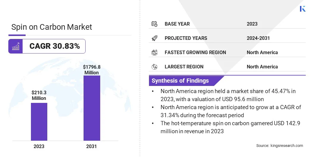
The global spin on carbon market size was valued at USD 210.3 million in 2023 and is projected to grow from USD 273.9 million in 2024 to USD 1796.8 million by 2031, exhibiting a CAGR of 30.83% during the forecast period.
Market growth is supported by increasing investment in semiconductor manufacturing worldwide. Governments and private sectors are expanding fabrication capacities to meet rising global demand for advanced chips used in artificial intelligence, automotive electronics, and high-speed connectivity.
These investments are highlighting the need for advanced materials such as spin on carbon that can meet the rigorous requirements of next-generation semiconductor production.
Major companies operating in the spin on carbon industry are Brewer Science, Inc., Merck KGaA, Shin-Etsu Chemical Co. LTD, Kayaku AM, DONGJIN SEMICHEM CO LTD., YCCHEM CO., Ltd., SAMSUNG, JSR Micro, Inc., Nano-C, and Irresistible Materials Ltd.
Moreover, the increasing use of spin on carbon in conjunction with EUV and next-generation lithography technologies is fueling market growth. As the transition to sub-5 nm nodes accelerates, spin on carbon materials are becoming vital for achieving high-precision multi-patterning and reliable etch masking.
Their strong film uniformity, heat resistance, and ability to withstand aggressive etching make them well-suited for intricate structures in logic, memory, and advanced packaging.
- In June 2024, Imec and ASML jointly launched the High NA EUV Lithography Lab in the Netherlands. This cutting-edge facility provides memory chip manufacturers and advanced materials and equipment suppliers access to the first the High NA EUV scanner prototype and a complete set of metrology and processing tools.
Key Highlights:
- The spin on carbon industry size was recorded at USD 210.3 million in 2023.
- The market is projected to grow at a CAGR of 30.83% from 2024 to 2031.
- North America held a share of 45.47% in 2023, valued at USD 95.6 million.
- The hot-temperature spin on carbon segment garnered USD 1204.0 million in revenue in 2023.
- The memory devices segment is expected to reach USD 554.9 million by 2031.
- The foundries segment is projected to generate a revenuwe of USD 984.7 million by 2031.
- Asia Pacific is anticipated to grow at a CAGR of 30.78% over the forecast period.
How are investments driving the market growth?
The spin on carbon market is experiencing significant growth, driven by increased investment in semiconductor manufacturing capacity. Governments and private sector players, particularly in regions such as North America and Asia Pacific, are making substantial investments to expand domestic semiconductor production.
This surge in investments is being fueled by the need to meet the growing global demand for advanced chips used in emerging technologies such as artificial intelligence, 5G, and cloud computing.
As semiconductor fabrication capacity expands to accommodate these new technologies, the demand for high-performance materials, including spin on carbon, is rising.
Spin on carbon materials are essential for meeting the advanced lithography and patterning requirements of modern semiconductor devices, making them critical to the production of smaller, more efficient chips.
- In April 2025, Applied Materials, Inc. purchased 9% of the outstanding shares of BE Semiconductor Industries N.V. (Besi). This initiative aims to co-develop the first fully integrated equipment solution for die-based hybrid bonding, a major technology for advanced semiconductor packaging.
What are the major obstacles for this market?
A key challenge hindering the expansion of the spin on carbon market is the complexity of integrating these materials into advanced semiconductor process nodes, particularly as manufacturing transitions to sub-5 nm technologies. At such scales, even minimal deviations in material properties can significantly impact yield, reliability, and overall process performance.
Achieving precise compatibility with etching, deposition, and cleaning steps becomes increasingly demanding, particularly within multilayered and three-dimensional device architectures. This issue is further intensified by the need for consistent film uniformity, high thermal stability, and ultra-low contamination levels.
This challenge can be addressed through collaboration between material suppliers and semiconductor manufacturers to co-develop spin on carbon solutions tailored to specific fabrication requirements.
Additionally, leveraging advanced modeling, real-time process monitoring, and predictive quality control technologies can help ensure consistent material behavior and accelerate time to market in high-volume production environments.
Which technological trends are shaping the market?
The spin on carbon market is witnessing a significant trend toward the integration of spin on carbon materials with extreme ultraviolet (EUV) and advanced lithography techniques.
As semiconductor manufacturers focus on sub-5 nm process nodes, the need for materials that can maintain structural integrity under demanding etch conditions and support fine pattern resolution has intensified.
Spin on carbon materials are gaining traction as reliable hardmask layers in these environments due to their superior etch selectivity and compatibility with complex multi-patterning processes.
Their ability to deliver reduced line edge roughness and support high-aspect ratio structures makes them particularly valuable in EUV workflows, where precision and process control are critical. This alignment with next-generation lithography technologies positions spin on carbon as a key enabler in advanced semiconductor fabrication.
- In April 2024, Intel Foundry, in collaboration with ASML, successfully installed and calibrated the industry’s first commercial High Numerical Aperture Extreme Ultraviolet (EUV) lithography tool at its R&D site in Hillsboro, Oregon. This represents a significant advancement in semiconductor manufacturing, enabling enhanced resolution and feature scaling for next-generation processors and supporting emerging technologies such as AI.
Spin on Carbon Market Report Snapshot
|
Segmentation
|
Details
|
|
By Material Type
|
Hot-temperature Spin on Carbon, Normal-temperature Spin on Carbon
|
|
By Application
|
Memory Devices, Logic Devices, Power Devices, Advanced Packaging, Photonics, MEMS
|
|
By End User
|
Foundries, Integrated Device Manufacturers (IDMs), Outsourced Semiconductor Assembly and Test (OSAT)
|
|
By Region
|
North America: U.S., Canada, Mexico
|
|
Europe: France, UK, Spain, Germany, Italy, Russia, Rest of Europe
|
|
Asia-Pacific: China, Japan, India, Australia, ASEAN, South Korea, Rest of Asia-Pacific
|
|
Middle East & Africa: Turkey, U.A.E., Saudi Arabia, South Africa, Rest of Middle East & Africa
|
|
South America: Brazil, Argentina, Rest of South America
|
Market Segmentation
- By Material Type (Hot-temperature Spin on Carbon and Normal-temperature Spin on Carbon): The hot-temperature spin on carbon segment earned USD 142.9 million in 2023 due to its superior thermal stability and suitability for advanced patterning in high-performance semiconductor processes.
- By Application (Memory Devices, Logic Devices, Power Devices, and Advanced Packaging): The memory devices segment held a share of 30.27% in 2023, fueled by increasing demand for high-density storage solutions in consumer electronics and data centers.
- By End User (Foundries, Integrated Device Manufacturers (IDMs) and Outsourced Semiconductor Assembly and Test (OSAT)): The foundries segment is projected to reach USD 984.7 million by 2031, propelled by growing investments in cutting-edge node technologies and volume production of advanced chips for global clients.
What is the market scenario in North America and Asia-Pacific region?
Based on region, the market has been classified into North America, Europe, Asia Pacific, Middle East & Africa, and Latin America.
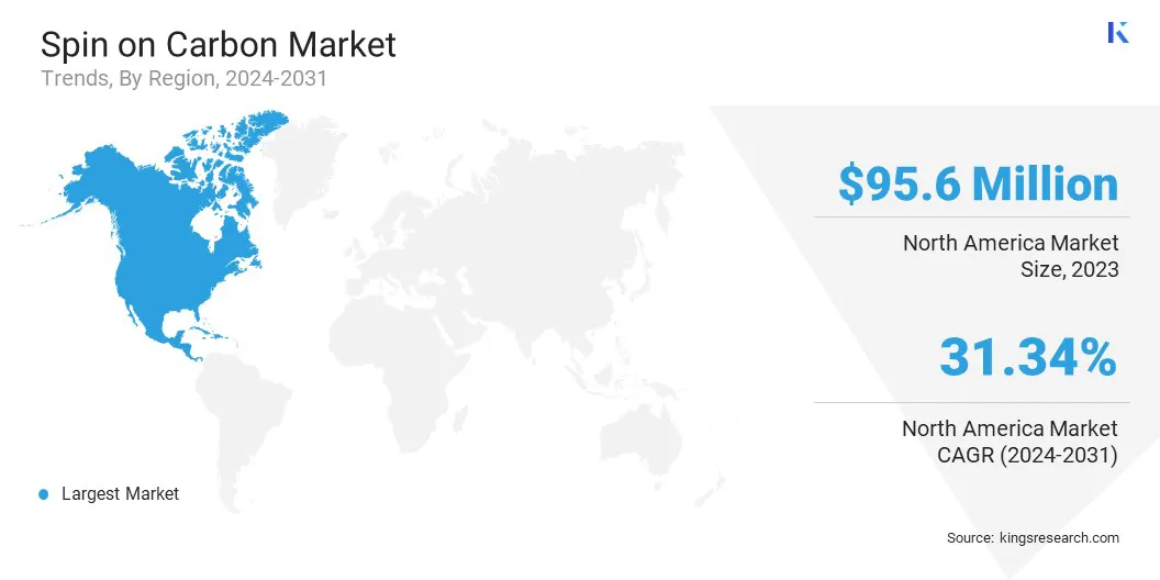
North America spin on carbon market share stood at around 45.47% in 2023, valued at USD 95.6 million. This dominance is attributed to the presence of well-established semiconductor manufacturers, advanced research infrastructure, and early adoption of cutting-edge lithography techniques.
Strong government support for domestic chip production and strategic investments in high-performance computing, artificial intelligence, and data center technologies are further contributing to regional market expansion.
The region has seen substantial investments in semiconductor manufacturing capabilities, with large-scale fabrication plant being built or expanded to support leading-edge nodes.
The United States, in particular, hosts several global semiconductor leaders and materials innovators that have been early adopters of spin on carbon materials for advanced lithography and etching.
- In March 2025, TSMC announced an additional USD 100 billion investment to expand its advanced semiconductor manufacturing operations in the U.S., supplementing its existing USD 65 billion investment in Phoenix, Arizona. The expansion includes two advanced packaging facilities, a cutting-edge R&D center, and new fabrication plants, making the largest foreign direct investment in U.S. history.
Asia Pacific spin on carbon industry is poised to grow at a staggering CAGR of 30.78% over the forecast period. This rapid growth is stimulated by the region’s expanding semiconductor fabrication capacity, particularly in countries such as South Korea, Taiwan, China, and Japan.
High demand for consumer electronics, growing adoption of advanced packaging, and continued investment in memory and logic device production are fueling regional market expansion. The presence of key material suppliers and a competitive manufacturing landscape further supports this growth.
Additionally, surging demand for consumer electronics, smartphones, and computing devices is aiding regional market expansion, all of which require increasingly compact and powerful semiconductor components.
As semiconductor nodes continue to shrink, spin on carbon plays a critical role in enabling precise lithographic patterning, particularlyin multi-patterning and 3D integration technologies.
Asia Pacific's strong presence in memory and logic chip production has further led to increased usage of spin on carbon in DRAM, NAND flash, and system-on-chip applications.
Regulatory Frameworks
- In the U.S, the regulatory framework for spin on carbon materials falls under the oversight of the Environmental Protection Agency (EPA) and the Occupational Safety and Health Administration (OSHA). These agencies set standards for air and water quality, hazardous materials handling, and worker safety in semiconductor manufacturing.
- In Europe, the European Chemicals Agency (ECHA) enforces the Registration, Evaluation, Authorisation, and Restriction of Chemicals (REACH) regulation, which governs the safe use and handling of chemicals, including those used in semiconductor processes like spin on carbon. REACH ensures that manufacturers provide safety data sheets and comply with environmental and safety standards.
Competitive Landscape
The spin on carbon industry is witnessing increased competition as companies intensify their efforts to enhance product performance, scale manufacturing, and support advanced semiconductor process nodes.
A common strategy among leading players involves expanding their R&D capabilities to develop next-generation spin on carbon formulations with improved etch resistance, thermal stability, and compatibility with extreme ultraviolet (EUV) and multi-patterning lithography.
Additionally, industry players are forming strategic collaborations with semiconductor foundries and device manufacturers. By engaging in joint development projects and early-stage material qualification programs, spin on carbon suppliers aim to align their offerings with specific process integration needs.
This enables faster adoption of their materials in volume production and strengthens their positioning within the semiconductor supply chain. In addition, market participants are priortizing geographic expansion through new manufacturing facilities or localized partnerships to support growing demand, particularly in Asia Pacific and North America.
Enhancing regional presence reduces lead times and logistics costs while also facilitating closer technical support for customers operating high-volume fabrication plants.
Top Companies in Spin on Carbon Market:
- Brewer Science, Inc.
- Merck KGaA
- Shin-Etsu Chemical Co. LTD
- Kayaku AM
- DONGJIN SEMICHEM CO LTD.
- YCCHEM CO.,Ltd.
- SAMSUNG
- JSR Micro, Inc.
- Nano-C
- Irresistible Materials Ltd
Recent Developments (Product Launch)
- In June 2023, Brewer Science, Inc. unveiled its breakthrough high-temperature stable gapfilling planarizing material, OptiStack SOC450. This advanced material provides zero shrinkage up to 550°C during N2 baking, revolutionizing advanced EUV and ArF processes by ensuring superior thermal stability and performance for planarization and gapfilling in next-generation semiconductor manufacturing.


